SNVS834 August   2014 LM3631

PRODUCTION DATA.  

  1. Features
  2. Applications
  3. Description
  4. Revision History
  5. Device Comparison Table
  6. Pin Configuration and Functions
  7. Specifications
    1. 7.1 Absolute Maximum Ratings
    2. 7.2 Handling Ratings
    3. 7.3 Recommended Operating Conditions
    4. 7.4 Thermal Information
    5. 7.5 Electrical Characteristics
    6. 7.6 I2C Timing Requirements (SDA, SCL)
    7. 7.7 Typical Characteristics
  8. Detailed Description
    1. 8.1 Overview
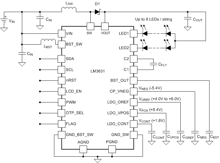
    2. 8.2 Functional Block Diagram
    3. 8.3 Features Description
      1. 8.3.1  Backlight
        1. 8.3.1.1 Backlight Brightness Control
          1. 8.3.1.1.1 LED Current With Brightness Selection '00'
          2. 8.3.1.1.2 LED Current With Brightness Selection '01'
          3. 8.3.1.1.3 LED Current With Brightness Selections '10' and '11'
        2. 8.3.1.2 Linear Slope and Advanced Slope
        3. 8.3.1.3 Mapper
        4. 8.3.1.4 PWM Detector and PWM Input
      2. 8.3.2  Backlight Boost Converter
        1. 8.3.2.1 Headroom Voltage
        2. 8.3.2.2 Automatic Switching Frequency Shift
        3. 8.3.2.3 Inductor Select Bit
        4. 8.3.2.4 PI-Compensator
      3. 8.3.3  Backlight Protection and Faults
        1. 8.3.3.1 Overvoltage Protection (OVP) and Open-Load Fault Protection
        2. 8.3.3.2 Overcurrent Protection (OCP) and Overcurrent Protection Fault
          1. 8.3.3.2.1 Overcurrent Protection Fault Flag (BL_OCPFLT)
          2. 8.3.3.2.2 Short Circuit Fault Flag (BL_SCFLT)
      4. 8.3.4  LCD Bias
        1. 8.3.4.1 Display Bias Power (VPOS, VNEG, VOREF)
        2. 8.3.4.2 Display Bias Power Sequencing (VPOS, VNEG, VOREF, VCONT)
          1. 8.3.4.2.1 Start-Up and Shutdown Delays
          2. 8.3.4.2.2 Special Conditions During Display Bias Power Sequencing
        3. 8.3.4.3 Active Discharge
        4. 8.3.4.4 LCD Bias Protection
      5. 8.3.5  Display Controller Power (VLDO_CONT)
      6. 8.3.6  RESET Register
      7. 8.3.7  nRST Input
      8. 8.3.8  FLAG Pin
      9. 8.3.9  Power-Good Flag
      10. 8.3.10 OTP_SEL Pin
      11. 8.3.11 Thermal Shutdown
      12. 8.3.12 Undervoltage Lockout
    4. 8.4 Device Functional Modes
      1. 8.4.1 Modes of Operation
    5. 8.5 Programming
      1. 8.5.1 I2C-Compatible Serial Bus Interface
        1. 8.5.1.1 Interface Bus Overview
        2. 8.5.1.2 Data Transactions
        3. 8.5.1.3 Acknowledge Cycle
        4. 8.5.1.4 Acknowledge After Every Byte Rule
        5. 8.5.1.5 Addressing Transfer Formats
    6. 8.6 Register Maps
  9. Application and Implementation
    1. 9.1 Application Information
    2. 9.2 Typical Application
      1. 9.2.1 Design Requirements
      2. 9.2.2 Detailed Design Procedure
        1. 9.2.2.1 External Components
        2. 9.2.2.2 Inductor Selection
        3. 9.2.2.3 Boost Output Capacitor Selection
        4. 9.2.2.4 Backlight Boost Diode Selection
        5. 9.2.2.5 Charge Pump Capacitor Selection
        6. 9.2.2.6 LDO Output Capacitor Selection
      3. 9.2.3 Application Curves
  10. 10Power Supply Recommendations
  11. 11Layout
    1. 11.1 Layout Guidelines
    2. 11.2 Layout Example
  12. 12Device and Documentation Support
    1. 12.1 Device Support
      1. 12.1.1 Third-Party Products Disclaimer
    2. 12.2 Trademarks
    3. 12.3 Electrostatic Discharge Caution
    4. 12.4 Glossary
  13. 13Mechanical, Packaging, and Orderable Information

Package Options

Mechanical Data (Package|Pins)
Thermal pad, mechanical data (Package|Pins)
Orderable Information

1 Features

  • Drives up to Two Strings with Maximum of Eight LEDs in Series
    • Integrated Backlight Boost with 29-V Maximum Output Voltage
    • Two Low-Side Constant-Current LED Drivers with 25-mA Maximum Output Current
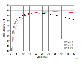
  • Backlight Efficiency Up to 90%
  • 11-Bit Linear or Exponential Dimming with up to 17-Bit Output Resolution
  • External PWM Input for CABC Backlight Operation
  • LCD Bias Efficiency > 85%
  • Programmable Positive LCD bias, 4-V to 6-V,
    100-mA Maximum Output Current
  • Programmable Negative LCD bias, –4-V to –6-V, 80-mA Maximum Output Current
  • Two Positive Programmable LDO Reference Outputs
    • 4-V to 6-V, 50-mA Maximum Output Current
    • 1.8-V to 3.3-V, 80-mA Maximum Output Current
  • 2.7-V to 5-V Input Voltage Range

2 Applications

    Mobile Device LCD Backlighting and Bias

3 Description

The LM3631 is a complete LCD backlight and bias power solution for mobile devices. This one-chip solution has an integrated high-efficiency backlight LED driver and positive/negative bias supplies for LCD drivers addressing the power requirements of high-definition LCDs. Integrated solution allows small solution size while still maintaining high performance.

Capable of driving up to 16 LEDs, the LM3631 is ideal for small- to medium-size displays. Two additional programmable LDO regulator outputs can be used to power display controller, LCD gamma reference, or any additional peripherals.

A high level of integration and programmability allows the LM3631 to address a variety of applications without the need for hardware changes. Voltage levels, backlight configuration, and power sequences are all configurable through I2C interface.

Device Information(1)

PART NUMBER PACKAGE BODY SIZE (MAX)
LM3631 DSBGA (24) 2.585 mm x 1.885 mm
  1. For all available packages, see the orderable addendum at the end of the datasheet.

Simplified Schematic

LM3631_Simplified_sch.gif

Backlight Efficiency, 2P6S

D007_SNVS834.gif