SNVSA63A April 2015 – September 2015 LM3632A
PRODUCTION DATA.
- 1 Features
- 2 Applications
- 3 Description
- 4 Revision History
- 5 Pin Configuration and Functions
- 6 Specifications
-
7 Detailed Description
- 7.1 Overview
- 7.2 Functional Block Diagram
- 7.3
Features Description
- 7.3.1 Backlight
- 7.3.2 LCM Bias
- 7.3.3 Flash
- 7.3.4 Software RESET
- 7.3.5 EN Input
- 7.3.6 Thermal Shutdown (TSD)
- 7.4 Device Functional Modes
- 7.5 Programming
- 7.6
Register Maps
- 7.6.1 Revision (Address = 0x01) [reset = 0x09]
- 7.6.2 Backlight Configuration1 (Address = 0x02) [reset = 0x30]
- 7.6.3 Backlight Configuration2 (Address = 0x03) [reset = 0x0D]
- 7.6.4 Backlight Brightness LSB (Address = 0x04) [reset = 0x07]
- 7.6.5 Backlight Brightness MSB (Address = 0x05) [reset = 0xFF]
- 7.6.6 Flash/Torch Current (Address = 0x06) [reset = 0x3E]
- 7.6.7 Flash Configuration (Address = 0x07) [reset = 0x2F]
- 7.6.8 VIN Monitor (Address = 0x08) [reset = 0x03]
- 7.6.9 I/O Control (Address = 0x09) [reset = 0x00]
- 7.6.10 Enable (Address = 0x0A) [reset = 0x00]
- 7.6.11 Flags1 (Address = 0x0B) [reset = 0x00]
- 7.6.12 Display Bias Configuration (Address = 0x0C) [reset = 0x18]
- 7.6.13 LCM Boost Bias (Address = 0x0D) [reset = 0x1E]
- 7.6.14 VPOS Bias (Address = 0x0E) [reset = 0x1E]
- 7.6.15 VNEG Bias (Address = 0x0F) [reset = 0x1C]
- 7.6.16 Flags2 (Address = 0x10) [reset = 0x00]
- 8 Application and Implementation
- 9 Power Supply Recommendations
- 10Layout
- 11Device and Documentation Support
- 12Mechanical, Packaging, and Orderable Information
Package Options
Mechanical Data (Package|Pins)
- YFF|30
Thermal pad, mechanical data (Package|Pins)
Orderable Information
1 Features
- Drives up to Two Strings of Typically Eight LEDs in Series
- Integrated Backlight Boost with 29-V Maximum Output Voltage
- Two Low-Side Constant-Current LED Drivers with 25-mA Maximum Output Current
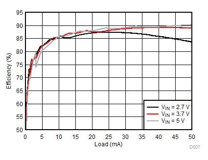
- Backlight Efficiency Up to 90%
- 11-Bit Exponential or Linear Dimming
- External PWM Input for CABC Backlight Operation
- LCD Bias Efficiency > 85%
- Programmable Positive LCD bias, 4-V to 6-V, 50-mA Maximum Output Current
- Programmable Negative LCD bias, –4-V to –6-V, 50-mA Maximum Output Current
- 1.5-A Flash LED Boost
- Flash Efficiency > 85%
- 2.7-V to 5-V Input Voltage Range
2 Applications
- Smart Phone LCD Backlighting and Bias
- Small Tablet LCD Backlighting and Bias
3 Description
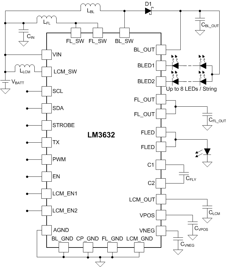
The LM3632A integrates the WLED drivers for both the backlight of the LCD panel and the camera flash along with the bias power for the LCD panel into one device. The device has all the safety features required in LED drivers with up to 90% efficiency and bias positive/negative power rails achieving 1.5% accuracy. Capable of driving up to 16 backlight LEDs, the device is ideal for small- to medium-size displays. A 1.5-A constant-current LED driver powered by a synchronous boost converter can be used for flash applications. The high-side flash current source allows for grounded cathode LED operation.
A high level of integration and programmability allows the LM3632A to address a variety of applications without the need for hardware changes.
Device Information(1)
| PART NUMBER | PACKAGE | BODY SIZE (MAX) |
|---|---|---|
| LM3632A | DSBGA (30) | 2.47 mm x 2.07 mm |
- For all available packages, see the orderable addendum at the end of the data sheet.
space
space
space
space
Simplified Schematic

Backlight Efficiency, 2P7S
