SNVS950C April 2014 – July 2016 LM5066I
PRODUCTION DATA.
- 1 Features
- 2 Applications
- 3 Description
- 4 Revision History
- 5 Device Comparison Table
- 6 Pin Configuration and Functions
- 7 Specifications
-
8 Detailed Description
- 8.1 Overview
- 8.2 Functional Block Diagram
- 8.3 Feature Description
- 8.4 Device Functional Modes
- 8.5
Programming
- 8.5.1 PMBus Command Support
- 8.5.2
Standard PMBus Commands
- 8.5.2.1 OPERATION (01h)
- 8.5.2.2 CLEAR_FAULTS (03h)
- 8.5.2.3 CAPABILITY (19h)
- 8.5.2.4 VOUT_UV_WARN_LIMIT (43h)
- 8.5.2.5 OT_FAULT_LIMIT (4Fh)
- 8.5.2.6 OT_WARN_LIMIT (51h)
- 8.5.2.7 VIN_OV_WARN_LIMIT (57h)
- 8.5.2.8 VIN_UV_WARN_LIMIT (58h)
- 8.5.2.9 STATUS_BYTE (78h)
- 8.5.2.10 STATUS_WORD (79h)
- 8.5.2.11 STATUS_VOUT (7Ah)
- 8.5.2.12 STATUS_INPUT (7Ch)
- 8.5.2.13 STATUS_TEMPERATURE (7dh)
- 8.5.2.14 STATUS_CML (7Eh)
- 8.5.2.15 STATUS_OTHER (7Fh)
- 8.5.2.16 STATUS_MFR_SPECIFIC (80h)
- 8.5.2.17 READ_EIN (86h)
- 8.5.2.18 READ_VIN (88h)
- 8.5.2.19 READ_IIN (89h)
- 8.5.2.20 READ_VOUT (8Bh)
- 8.5.2.21 READ_TEMPERATURE_1 (8Dh)
- 8.5.2.22 READ_PIN (97h)
- 8.5.2.23 MFR_ID (99h)
- 8.5.2.24 MFR_MODEL (9Ah)
- 8.5.2.25 MFR_REVISION (9Bh)
- 8.5.3
Manufacturer Specific PMBus Commands
- 8.5.3.1 MFR_SPECIFIC_00: READ_VAUX (D0h)
- 8.5.3.2 MFR_SPECIFIC_01: MFR_READ_IIN (D1h)
- 8.5.3.3 MFR_SPECIFIC_02: MFR_READ_PIN (D2h)
- 8.5.3.4 MFR_SPECIFIC_03: MFR_IN_OC_WARN_LIMIT (D3h)
- 8.5.3.5 MFR_SPECIFIC_04: MFR_PIN_OP_WARN_LIMIT (D4h)
- 8.5.3.6 MFR_SPECIFIC_05: READ_PIN_PEAK (D5h)
- 8.5.3.7 MFR_SPECIFIC_06: CLEAR_PIN_PEAK (D6h)
- 8.5.3.8 MFR_SPECIFIC_07: GATE_MASK (D7h)
- 8.5.3.9 MFR_SPECIFIC_08: ALERT_MASK (D8h)
- 8.5.3.10 MFR_SPECIFIC_09: DEVICE_SETUP (D9h)
- 8.5.3.11 MFR_SPECIFIC_10: BLOCK_READ (DAh)
- 8.5.3.12 MFR_SPECIFIC_11: SAMPLES_FOR_AVG (DBh)
- 8.5.3.13 MFR_SPECIFIC_12: READ_AVG_VIN (DCh)
- 8.5.3.14 MFR_SPECIFIC_13: READ_AVG_VOUT (DDh)
- 8.5.3.15 MFR_SPECIFIC_14: READ_AVG_IIN (DEh)
- 8.5.3.16 MFR_SPECIFIC_14: READ_AVG_PIN (DFh)
- 8.5.3.17 MFR_SPECIFIC_15: READ_AVG_PIN
- 8.5.3.18 MFR_SPECIFIC_16: BLACK_BOX_READ (E0h)
- 8.5.3.19 MFR_SPECIFIC_17: READ_DIAGNOSTIC_WORD (E1h)
- 8.5.3.20 MFR_SPECIFIC_18: AVG_BLOCK_READ (E2h)
- 8.5.4 Reading and Writing Telemetry Data and Warning Thresholds
- 8.5.5 Determining Telemetry Coefficients Empirically With Linear Fit
- 8.5.6 Writing Telemetry Data
- 8.5.7 PMBus Address Lines (ADR0, ADR1, ADR2)
- 8.5.8 SMBA Response
-
9 Application and Implementation
- 9.1 Application Information
- 9.2
Typical Application
- 9.2.1
48-V, 10-A PMBus Hotswap Design
- 9.2.1.1 Design Requirements
- 9.2.1.2
Detailed Design-In Procedure
- 9.2.1.2.1 Select RSNS and CL Setting
- 9.2.1.2.2 Selecting the Hotswap FETs
- 9.2.1.2.3 Select Power Limit
- 9.2.1.2.4 Set Fault Timer
- 9.2.1.2.5 Check MOSFET SOA
- 9.2.1.2.6 Set UVLO and OVLO Thresholds
- 9.2.1.2.7 Power Good Pin
- 9.2.1.2.8 Input and Output Protection
- 9.2.1.2.9 Final Schematic and Component Values
- 9.2.1.3 Application Curves
- 9.2.2
48-V, 20-A PMBus Hotswap Design
- 9.2.2.1 Design Requirements
- 9.2.2.2
Detailed Design Procedure
- 9.2.2.2.1 Selecting the Sense Resistor and CL Setting
- 9.2.2.2.2 Selecting the Hotswap FETs
- 9.2.2.2.3 Select Power Limit
- 9.2.2.2.4 Set Fault Timer
- 9.2.2.2.5 Check MOSFET SOA
- 9.2.2.2.6 Switching to dv/dt-Based Start-Up
- 9.2.2.2.7 Choosing the VOUT Slew Rate
- 9.2.2.2.8 Select Power Limit and Fault Timer
- 9.2.2.2.9 Chose Input and Output Protection and Set Undervoltage, Overvoltage, and Power Good Thresholds
- 9.2.2.2.10 Final Schematic and Component Values
- 9.2.2.3 Application Curves
- 9.2.1
48-V, 10-A PMBus Hotswap Design
- 10Power Supply Recommendations
- 11Layout
- 12Device and Documentation Support
- 13Mechanical, Packaging, and Orderable Information
Package Options
Mechanical Data (Package|Pins)
- PWP|28
Thermal pad, mechanical data (Package|Pins)
- PWP|28
Orderable Information
1 Features
- 10- to 80-V Operation
- 100-V Continuous Absolute Max
- 26 mV or 50 mV ILIM Threshold (±10%)
- Programmable FET SOA Protection
- Programable UV, OV, tFAULT Thresholds
- External FET Temperature Sensing
- Failed FET Detection
- I2C / SMBus Interface
- PMBus™ and Node Manager 2.0 and 3.0 Compliant Command Structure
- Precision V IN, VOUT, IIN, PIN, VAUX Monitoring
- V (±1.25%); I (±1.75%); P (±2.5%)
- Supports Energy Monitoring via Read_EIN Command
- Programable I/V/P Averaging Interval
- 12-bit ADC with 1-kHz Sampling Rate
- –40°C < TJ < 125°C Operation
2 Applications
- 48-V Servers
- Base Station Power Distribution
- Networking Routers and Switchers
- PLC Power Management
- 24- to 28-V Industrial Systems
3 Description
LM5066I provides robust protection and precision monitoring for 10- to 80-V systems. Programmable UV, OV, ILIMIT, and fast-short circuit protection allow for customized protection for any application. Programmable FET SOA protection sets the maximum power the FET is allowed to dissipate under any condition. The programmable fault timer (tFAULT) is set to avoid nuisance trips, ensure start-up, and limit the duration of over load events.
In addition to circuit protection, the LM5066I supplies real-time power, voltage, current, temperature, and fault data to the system management host through the I2C / SMBus interface. PMBus compliant command structure makes it easy to program the device. Precision telemetry enables intelligent power management functions such as efficiency optimization and early fault detection. LM5066I also supports advanced features such as I/V/P averaging and peak power measurment to improve system diagnostics.
LM5066I is pin-to-pin compatible with the LM5066 and offers improved telemetry accuracy and supports the Read_Ein command to monitor energy. See Table 1 for a detailed comparison.
Device Information(1)
| PART NUMBER | PACKAGE | BODY SIZE (NOM) |
|---|---|---|
| LM5066I | PWP (28) | 9.70 × 4.40 mm2 |
SPACE
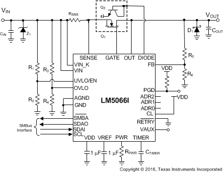
Simplified Schematic

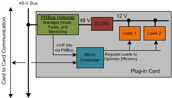
LM5066I in a Plug-in Card
