SNOSD60 June   2017 LMC6001-MIL

PRODUCTION DATA.  

  1. Features
  2. Applications
  3. Description
  4. Pin Configuration and Functions
  5. Specifications
    1. 5.1 Absolute Maximum Ratings
    2. 5.2 ESD Ratings
    3. 5.3 Recommended Operating Conditions
    4. 5.4 Thermal Information
    5. 5.5 DC Electrical Characteristics for LMC6001AI
    6. 5.6 Dissipation Ratings
    7. 5.7 Typical Characteristics
  6. Detailed Description
    1. 6.1 Overview
    2. 6.2 Functional Block Diagram
    3. 6.3 Feature Description
      1. 6.3.1 Amplifier Topology
      2. 6.3.2 Latch-up Prevention
    4. 6.4 Device Functional Modes
  7. Applications and Implementation
    1. 7.1 Application Information
      1. 7.1.1 Compensating for Input Capacitance
      2. 7.1.2 Capacitive Load Tolerance
    2. 7.2 Typical Application
      1. 7.2.1 Two Op Amp, Temperature Compensated Ph Probe Amplifier
        1. 7.2.1.1 Design Requirements
        2. 7.2.1.2 Detailed Design Procedure
        3. 7.2.1.3 Application Curve
    3. 7.3 System Example
      1. 7.3.1 Ultra-Low Input Current Instrumentation Amplifier
  8. Power Supply Recommendations
  9. Layout
    1. 9.1 Layout Guidelines
      1. 9.1.1 Printed-Circuit-Board Layout For High-Impedance Work
    2. 9.2 Layout Example
  10. 10Device and Documentation Support
    1. 10.1 Documentation Support
      1. 10.1.1 Related Documentation
    2. 10.2 Related Links
    3. 10.3 Community Resources
    4. 10.4 Trademarks
    5. 10.5 Electrostatic Discharge Caution
    6. 10.6 Glossary
  11. 11Mechanical, Packaging, and Orderable Information

Package Options

Mechanical Data (Package|Pins)
  • Y|0
Thermal pad, mechanical data (Package|Pins)
Orderable Information

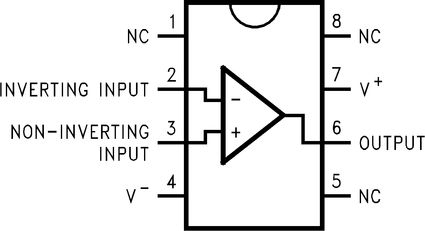
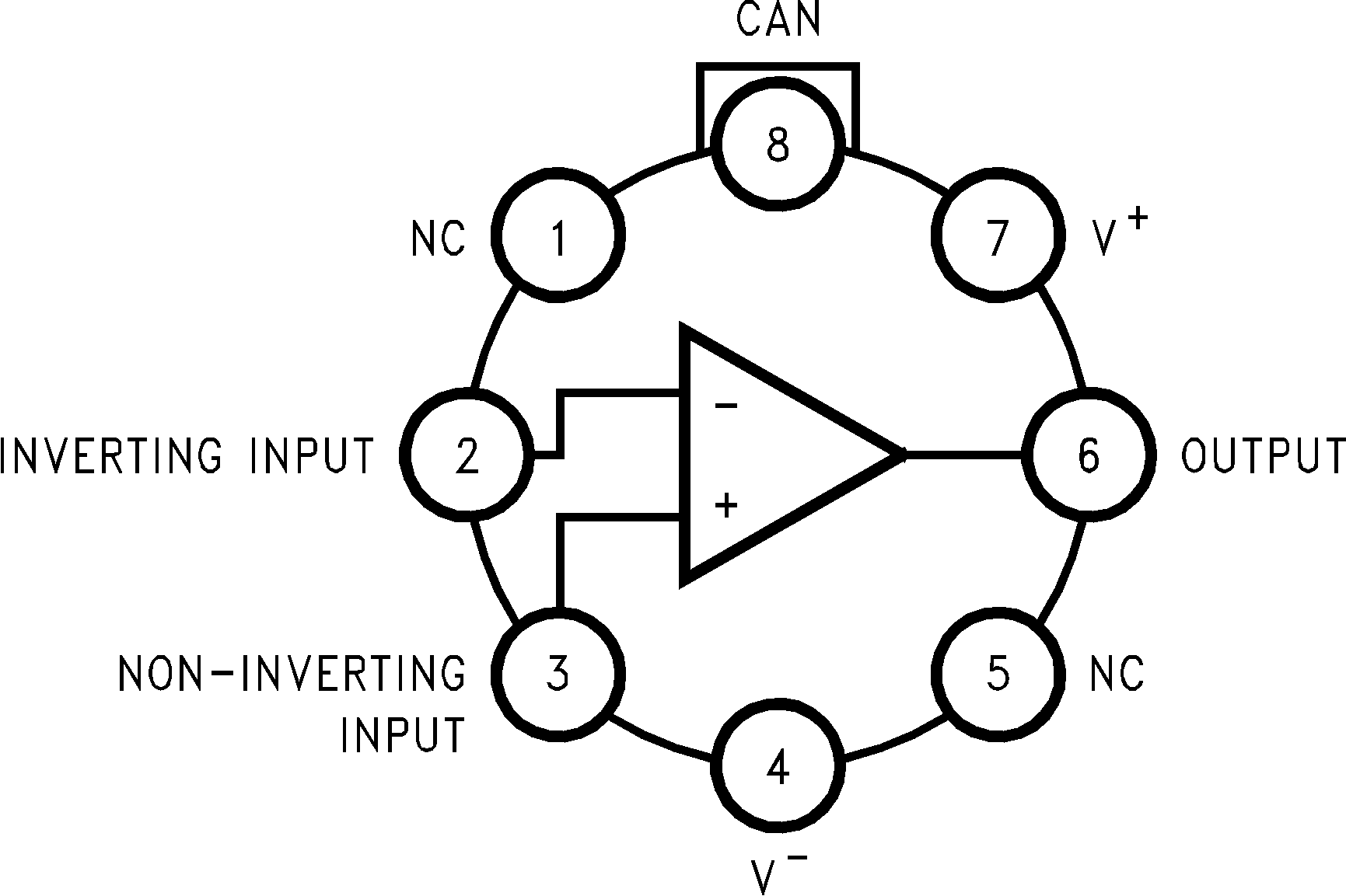
Pin Configuration and Functions

P Package
8-Pin PDIP
Top View
LMC6001-MIL 1188701.png
LMC Package
8-Pin TO-99
Top View
LMC6001-MIL 1188702.png

Pin Functions

PIN I/O DESCRIPTION
NAME PDIP NO. TO-99 NO.
CAN 8 No internal connection; connected to the external casing.
+IN 3 3 I Noninverting Input
–IN 2 2 I Inverting Input
NC 1, 5, 8 1, 5 No connection
OUTPUT 6 6 O Output
V+ 7 7 Positive (higher) power supply
V– 4 4 Negative (lower) power supply