SNOSD60 June 2017 LMC6001-MIL
PRODUCTION DATA.
- 1 Features
- 2 Applications
- 3 Description
- 4 Pin Configuration and Functions
- 5 Specifications
- 6 Detailed Description
- 7 Applications and Implementation
- 8 Power Supply Recommendations
- 9 Layout
- 10Device and Documentation Support
- 11Mechanical, Packaging, and Orderable Information
Package Options
Mechanical Data (Package|Pins)
- Y|0
Thermal pad, mechanical data (Package|Pins)
Orderable Information
5 Specifications
5.1 Absolute Maximum Ratings
Over operating free-air temperature range (unless otherwise noted)(1)(2)| MIN | MAX | Unit | |
|---|---|---|---|
| Differential Input Voltage | ±Supply Voltage | ||
| Voltage at Input/Output Pin | (V+) + 0.3 | (V−) − 0.3 | V |
| Supply Voltage (V+ − V−) | −0.3 | +16 | V |
| Output Short Circuit to V+ | See (3)(4) | ||
| Output Short Circuit to V− | See (3) | ||
| Lead Temperature (Soldering, 10 Sec.) | 260 | °C | |
| Junction Temperature | 150 | °C | |
| Current at Input Pin | ±10 | mA | |
| Current at Output Pin | ±30 | mA | |
| Current at Power Supply Pin | 40 | mA | |
| Storage Temperature, Tstg | −65 | 150 | °C |
(1) Stresses beyond those listed under Absolute Maximum Ratings may cause permanent damage to the device. These are stress ratings only, which do not imply functional operation of the device at these or any other conditions beyond those indicated under Recommended Operating Conditions. Exposure to absolute-maximum-rated conditions for extended periods may affect device reliability.
(2) If Military/Aerospace specified devices are required, please contact the Texas Instruments Sales Office/ Distributors for availability and specifications.
(3) Applies to both single supply and split supply operation. Continuous short circuit operation at elevated ambient temperature can result in exceeding the maximum allowed junction temperature of 150°C. Output currents in excess of ±30 mA over long term may adversely affect reliability.
(4) Do not connect the output to V+, when V+ is greater than 13 V or reliability will be adversely affected.
5.2 ESD Ratings
| VALUE | UNIT | |||
|---|---|---|---|---|
| V(ESD) | Electrostatic discharge | Human body model (HBM), per ANSI/ESDA/JEDEC JS-001(1)(2) | ±2000 | V |
(1) JEDEC document JEP155 states that 500-V HBM allows safe manufacturing with a standard ESD control process.
(2) Human body model, 1.5 kΩ in series with 100 pF.
5.3 Recommended Operating Conditions
Over operating free-air temperature range (unless otherwise noted).| MIN | MAX | UNIT | |||
|---|---|---|---|---|---|
| VSS | Supply input voltage | 4.5 | 15.5 | V | |
| TJ | Operating junction temperature | –40 | 85 | °C | |
5.4 Thermal Information
| THERMAL METRIC(1) | LMC6001-MIL | UNIT | ||
|---|---|---|---|---|
| P (PDIP) | LMC (TO-99) | |||
| 8 PINS | 8 PINS | |||
| RθJA | Junction-to-ambient thermal resistance | 100 | 145 | °C/W |
| RθJC(top) | Junction-to-case (top) thermal resistance | — | 45 | °C/W |
(1) For more information about traditional and new thermal metrics, see the Semiconductor and IC Package Thermal Metrics application report, SPRA953.
5.5 DC Electrical Characteristics for LMC6001AI
Limits are ensured for TJ = 25°C unless otherwise specified. Unless otherwise specified, V+ = 5 V, V− = 0 V, VCM = 1.5 V, and RL > 1 M.| PARAMETER | TEST CONDITIONS | LMC6001AI | UNIT | |||||
|---|---|---|---|---|---|---|---|---|
| MIN(2) | TYP(1) | MAX(2) | ||||||
| IB | Input Current | Either Input, VCM = 0 V, VS = ±5 V | 10 | 25 | fA | |||
| At the temperature extremes | 2000 | |||||||
| IOS | Input Offset Current | 5 | ||||||
| At the temperature extremes | 1000 | |||||||
| VOS | Input Offset Voltage | 0.7 | mV | |||||
| At the temperature extremes | 1 | |||||||
| VS = ±5 V, VCM = 0 V | 10 | |||||||
| At the temperature extremes | 1.35 | |||||||
| TCVOS | Input Offset Voltage Drift | 2.5 | µV/°C | |||||
| RIN | Input Resistance | >1 | TΩ | |||||
| CMRR | Common Mode | 0 V ≤ VCM ≤ 7.5 V | 75 | 83 | dB | |||
| Rejection Ratio | V+ = 10 V | At the temperature extremes | 72 | |||||
| +PSRR | Positive Power Supply Rejection Ratio | 5 V ≤ V+ ≤ 15 V | 73 | 83 | ||||
| At the temperature extremes | 70 | |||||||
| −PSRR | Negative Power Supply Rejection Ratio | 0 V ≥ V− ≥ −10 V | 80 | 94 | ||||
| At the temperature extremes | 77 | |||||||
| AV | Large Signal Voltage Gain | Sourcing, RL = 2 kΩ(3) | 400 | 1400 | V/mV | |||
| 300 | ||||||||
| Sinking, RL = 2 kΩ(3) | 180 | 350 | ||||||
| At the temperature extremes | 100 | |||||||
| VCM | Input Common-Mode Voltage | V+ = 5 V and 15 V For CMRR ≥ 60 dB | VCM Low | –0.4 | –0.1 | V | ||
| At the temperature extremes | 0 | |||||||
| VCM High | V+ − 2.3 | V+ − 1.9 | ||||||
| At the temperature extremes | V+ − 2.5 | |||||||
| VO | Output Swing | V+ = 15 V, RL = 2 kΩ to 2.5 V | VO Low | 0.1 | 0.14 | V | ||
| At the temperature extremes | 0.17 | |||||||
| VO High | 4.8 | 4.87 | ||||||
| At the temperature extremes | 4.73 | |||||||
| V+ = 15 V, RL = 2 kΩ to 7.5 V | VO Low | 0.26 | 0.35 | |||||
| At the temperature extremes | 0.45 | |||||||
| VO High | 14.5 | 14.63 | ||||||
| At the temperature extremes | 14.34 | |||||||
| IO | Output Current | Sourcing, V+ = 5 V, VO = 0 V |
16 | 22 | mA | |||
| At the temperature extremes | 10 | |||||||
| Sinking, V+ = 5 V, VO = 5 V |
16 | 21 | ||||||
| At the temperature extremes | 13 | |||||||
| Sourcing, V+ = 15 V, VO = 0 V |
28 | 30 | ||||||
| At the temperature extremes | 22 | |||||||
| Sinking, V+ = 15 V, VO = 13 V(4) |
28 | 34 | ||||||
| At the temperature extremes | 22 | |||||||
| IS | Supply Current | V+ = 5 V, VO = 1.5 V | 450 | 750 | µA | |||
| At the temperature extremes | 900 | |||||||
| V+ = 15 V, VO = 7.5 V | 550 | 850 | ||||||
| At the temperature extremes | 950 | |||||||
(1) Typical values represent the most likely parametric norm.
(2) All limits are specified by testing or statistical analysis.
(3) V+ = 15 V, VCM = 7.5 V and RL connected to 7.5 V. For Sourcing tests, 7.5 V ≤ VO ≤ 11.5 V. For Sinking tests, 2.5 V ≤ VO ≤ 7.5 V.
(4) Do not connect the output to V + , when V + is greater than 13 V or reliability will be adversely affected.
5.6 Dissipation Ratings
| MIN | MAX | UNIT | ||
|---|---|---|---|---|
| Power Dissipation | See (1) | |||
(1) For operating at elevated temperatures the device must be derated based on the thermal resistance θJA with PD = (TJ − TA)/θJA.
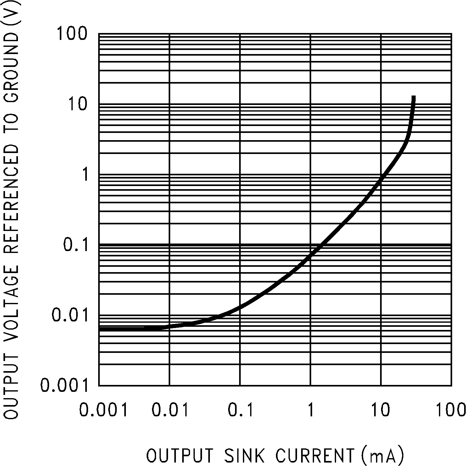
5.7 Typical Characteristics
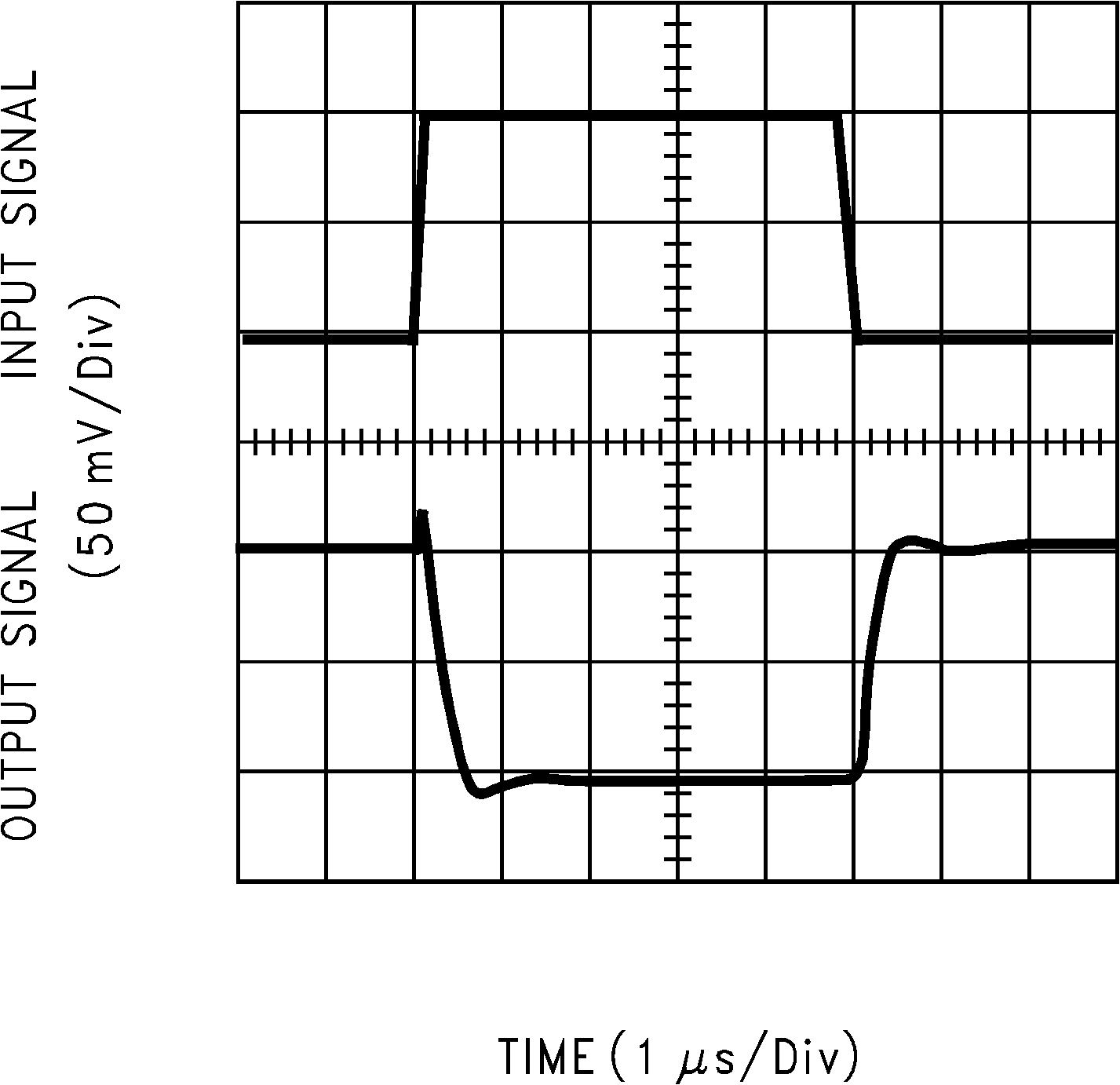
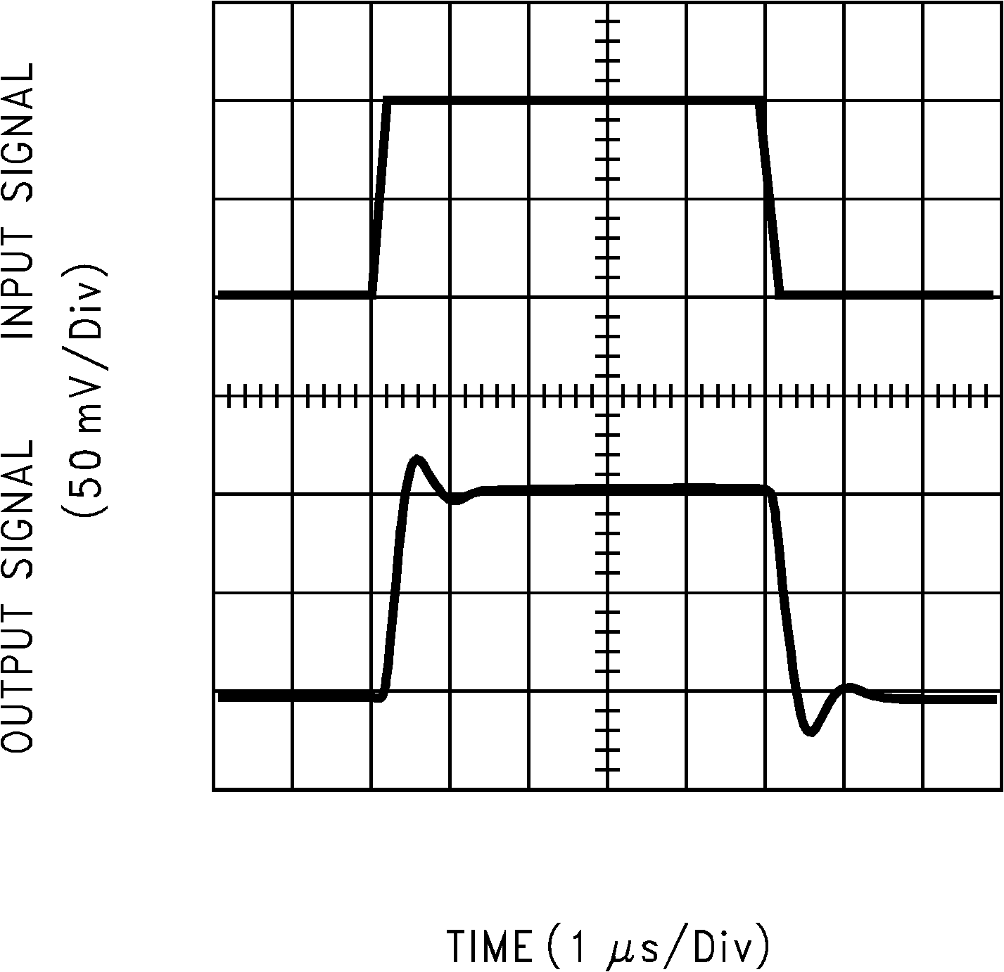
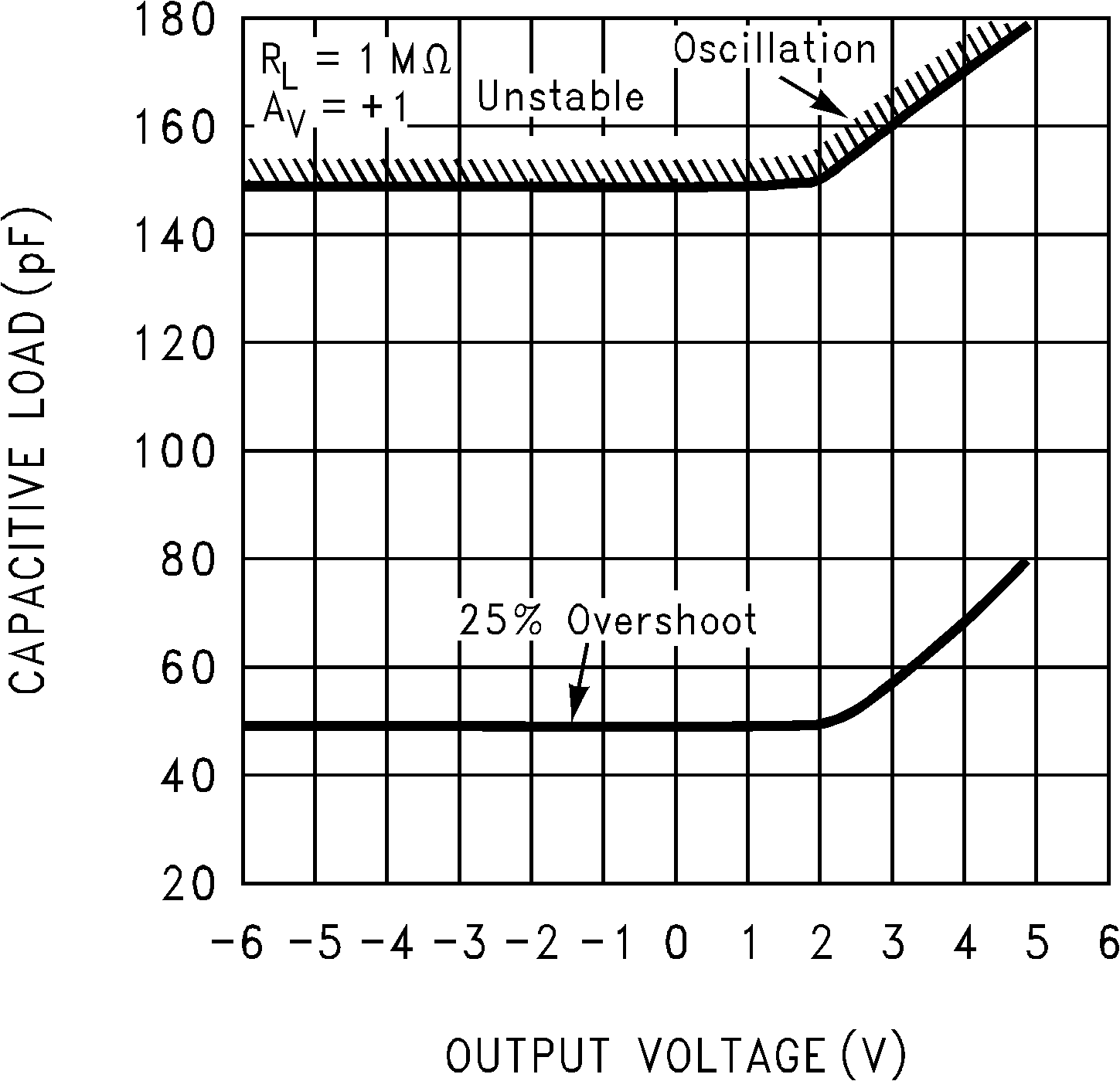
VS = ±7.5 V, TA = 25°C, unless otherwise specified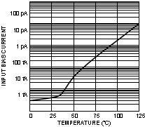
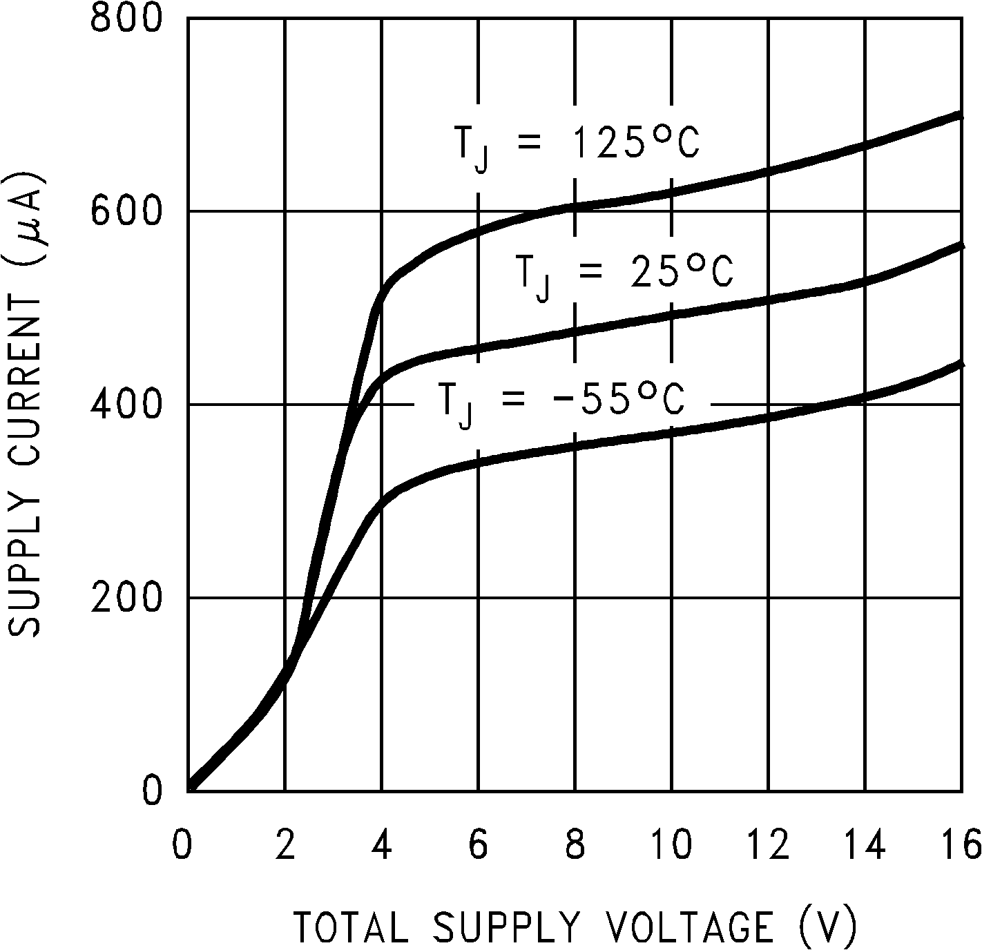
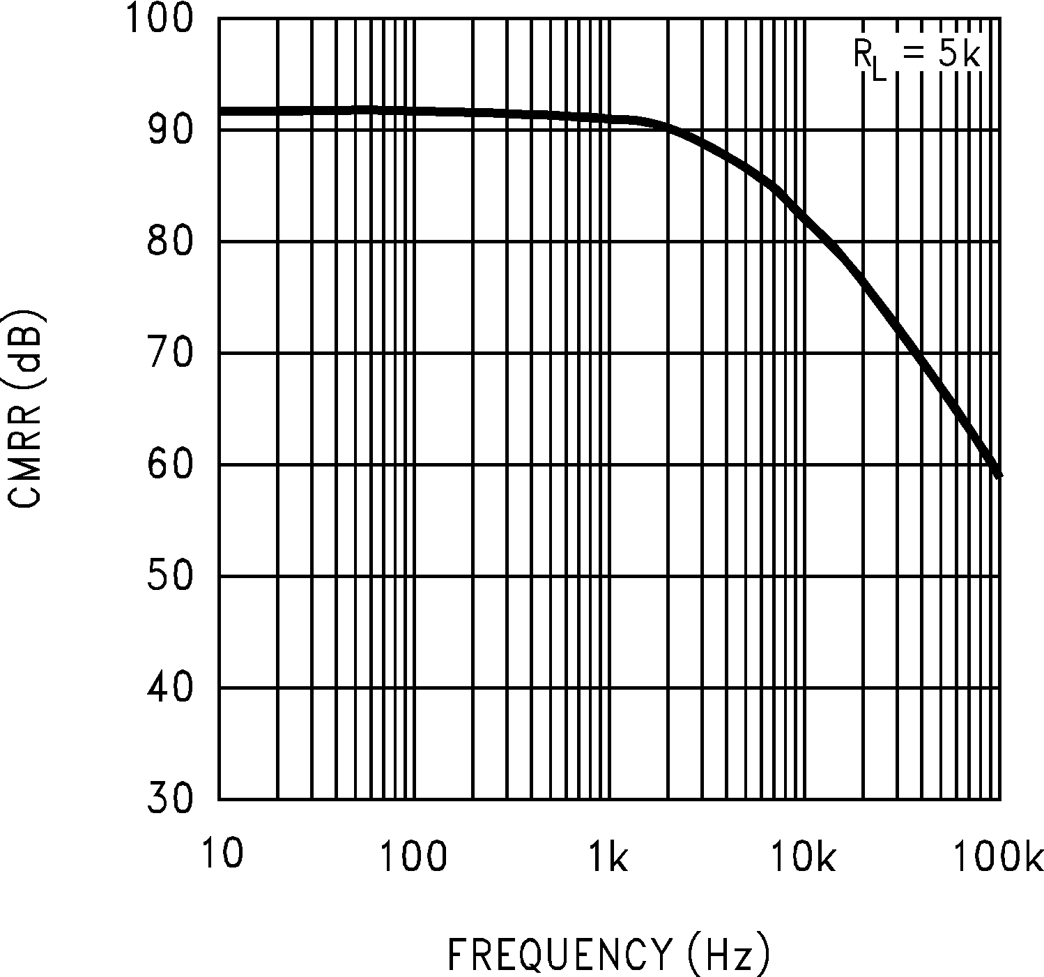
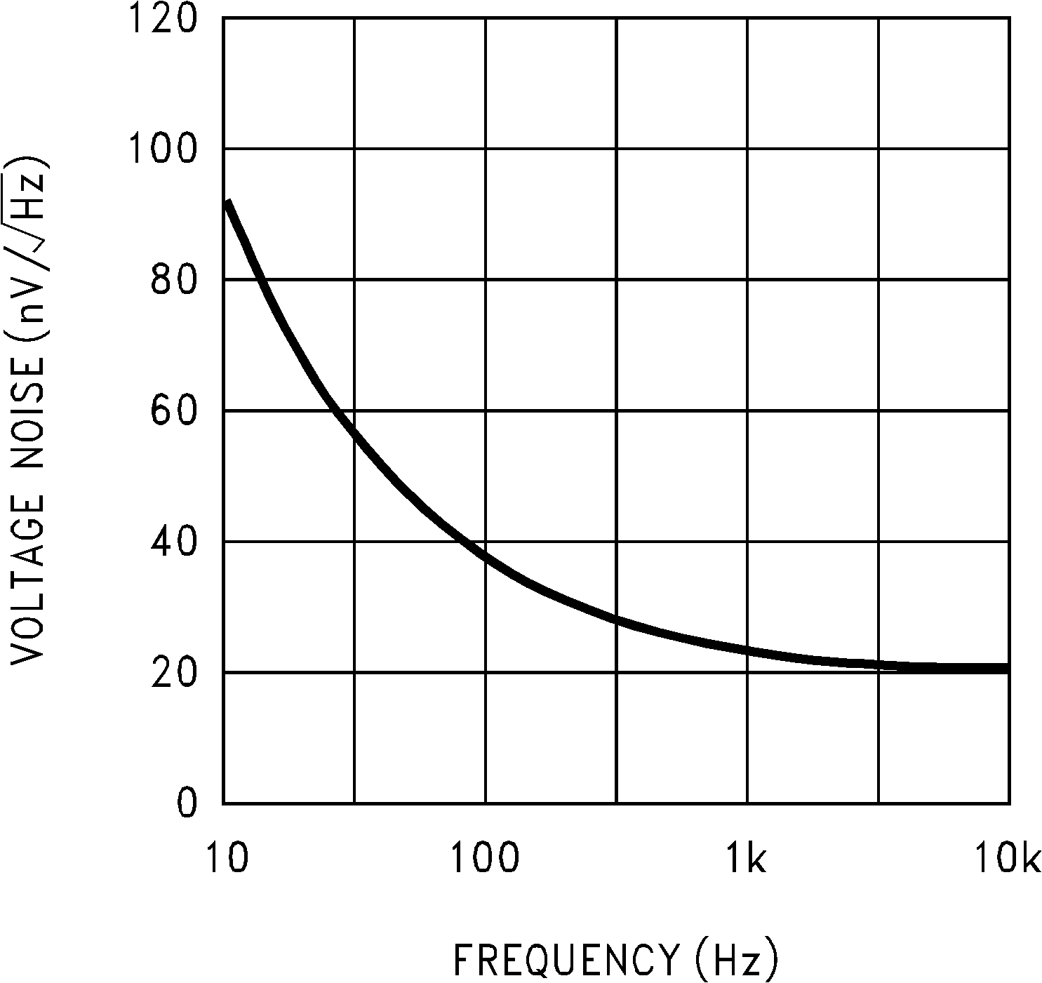
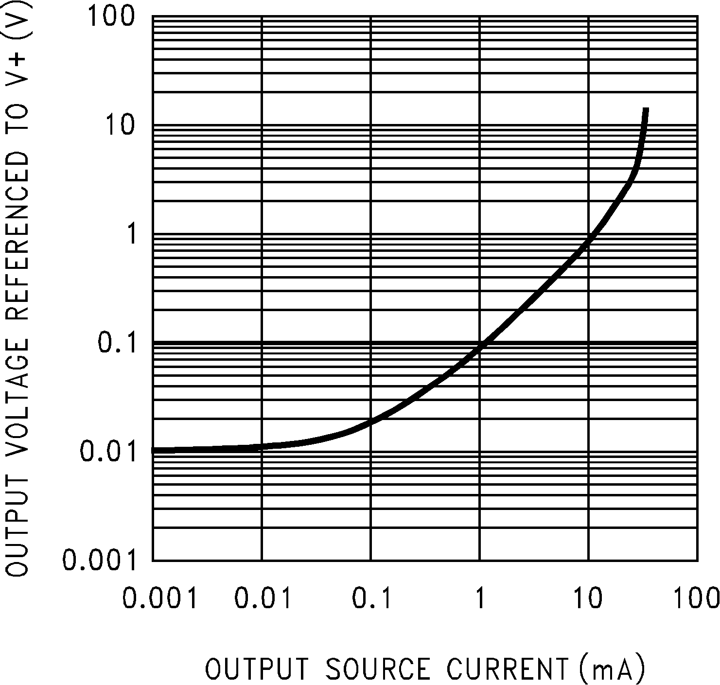
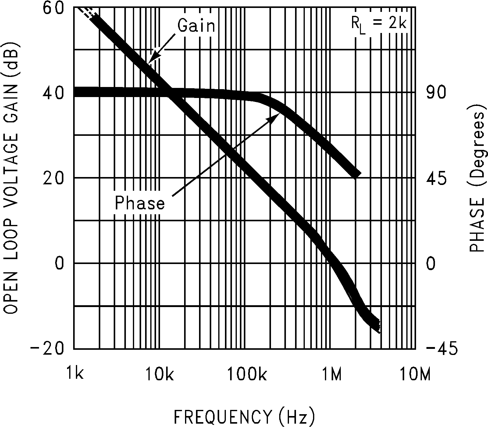
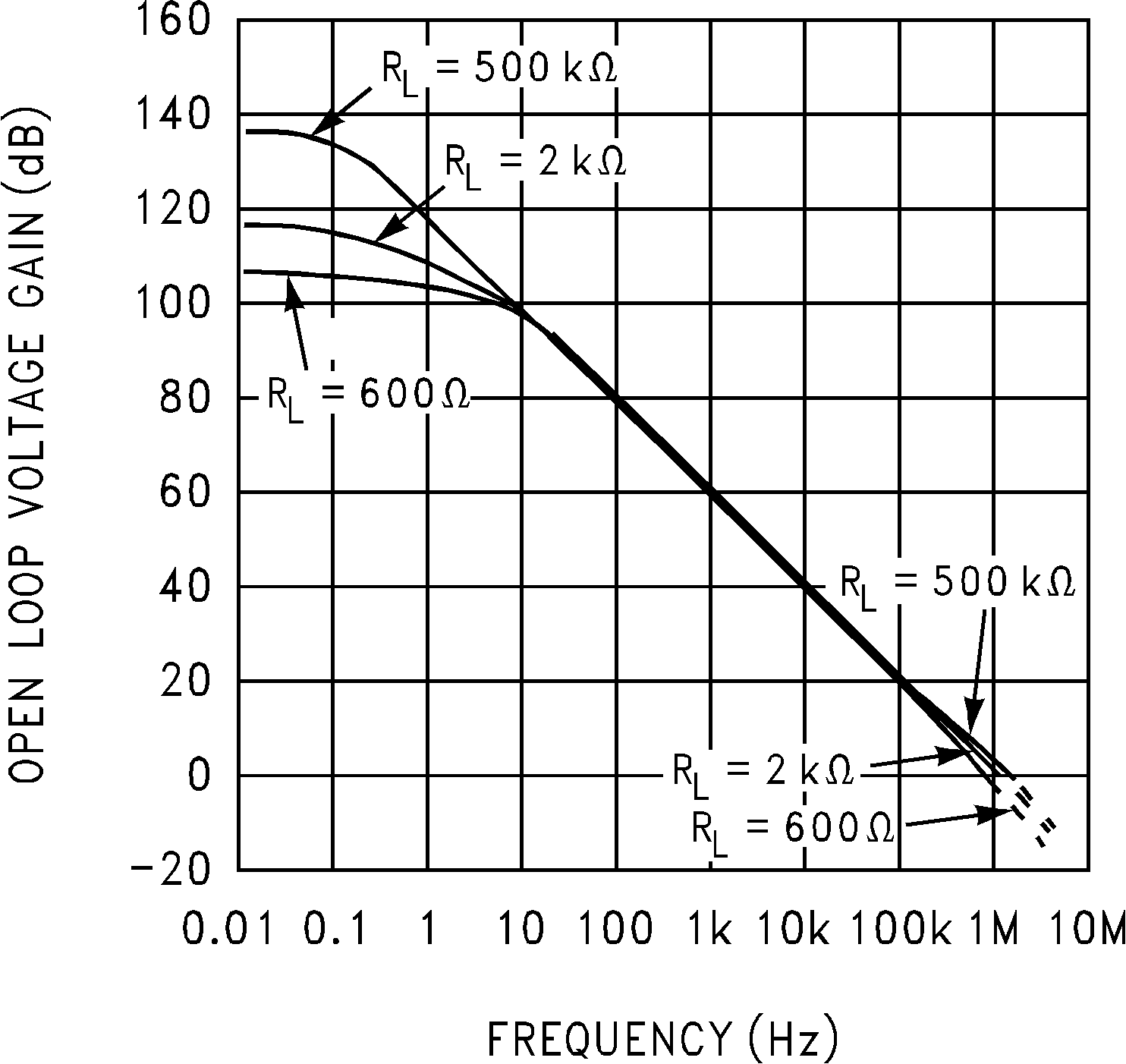
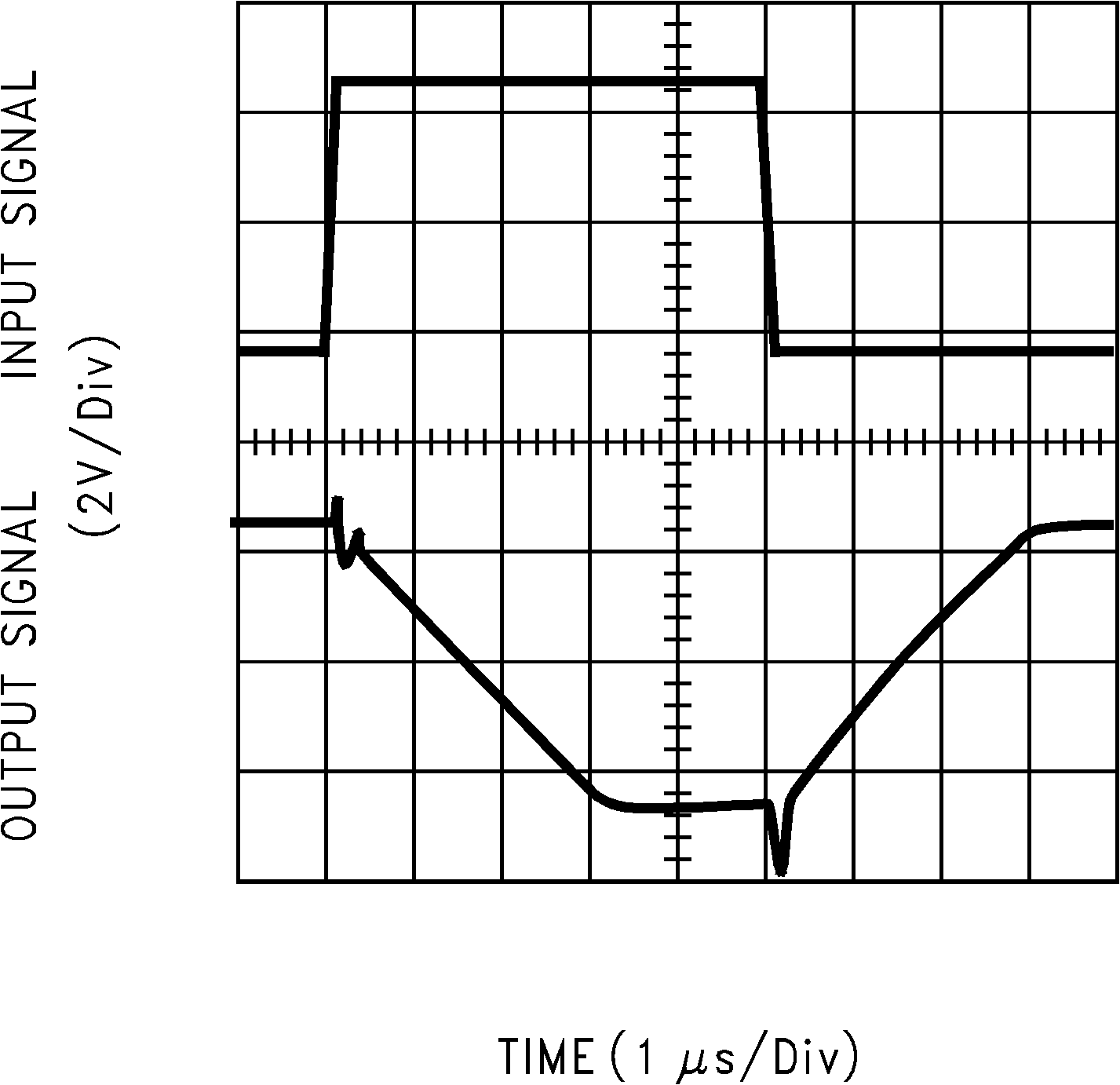
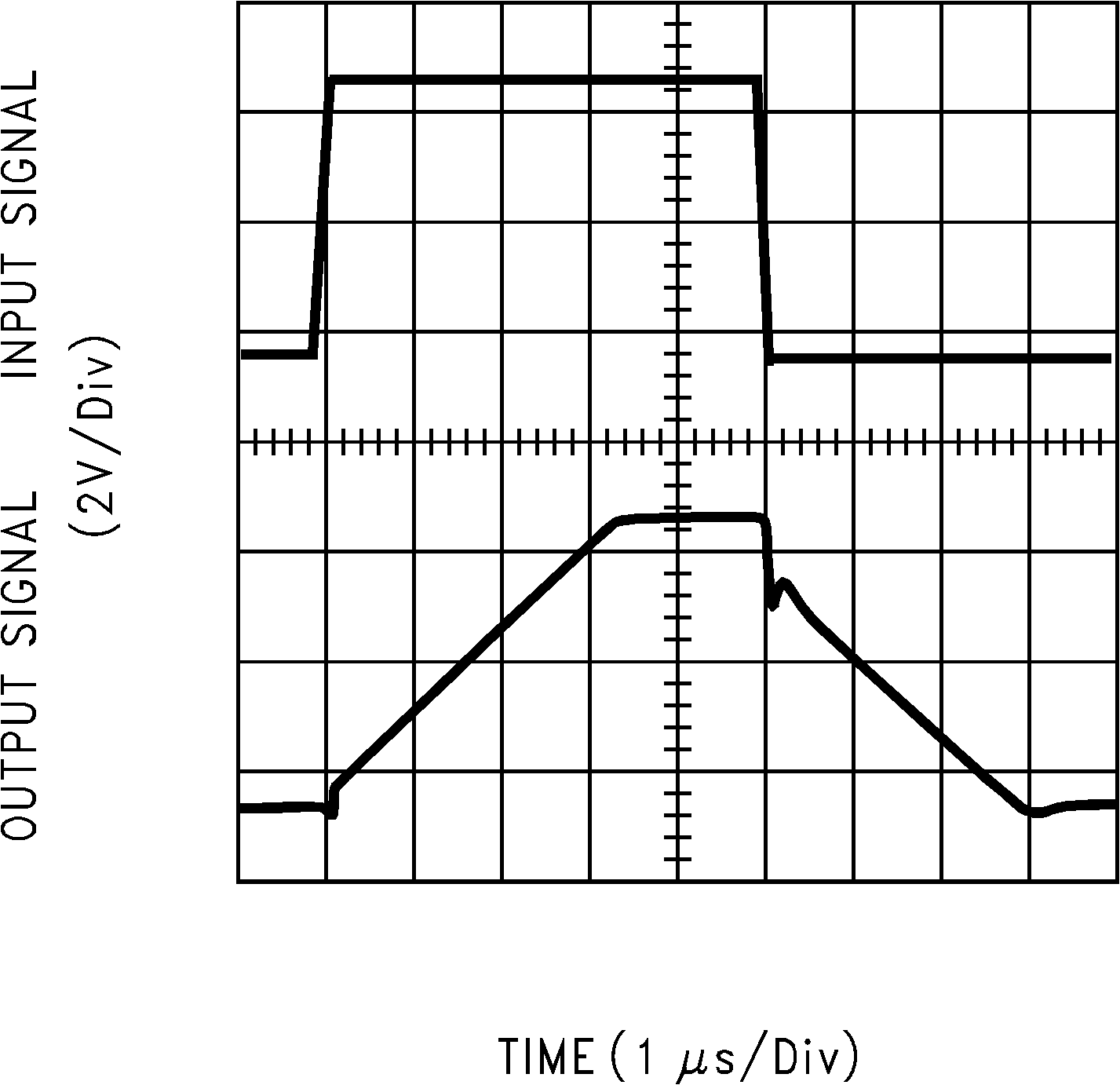
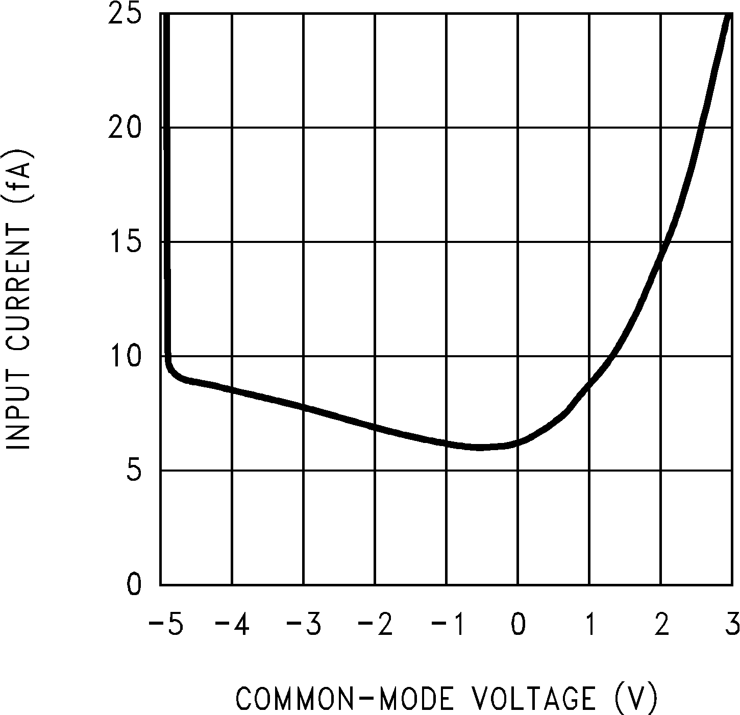
| VS = ±5 V | ||
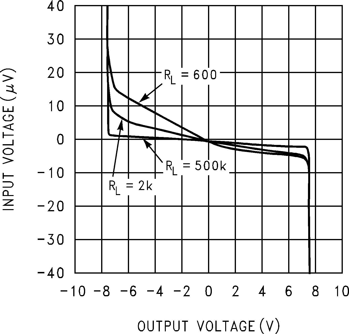
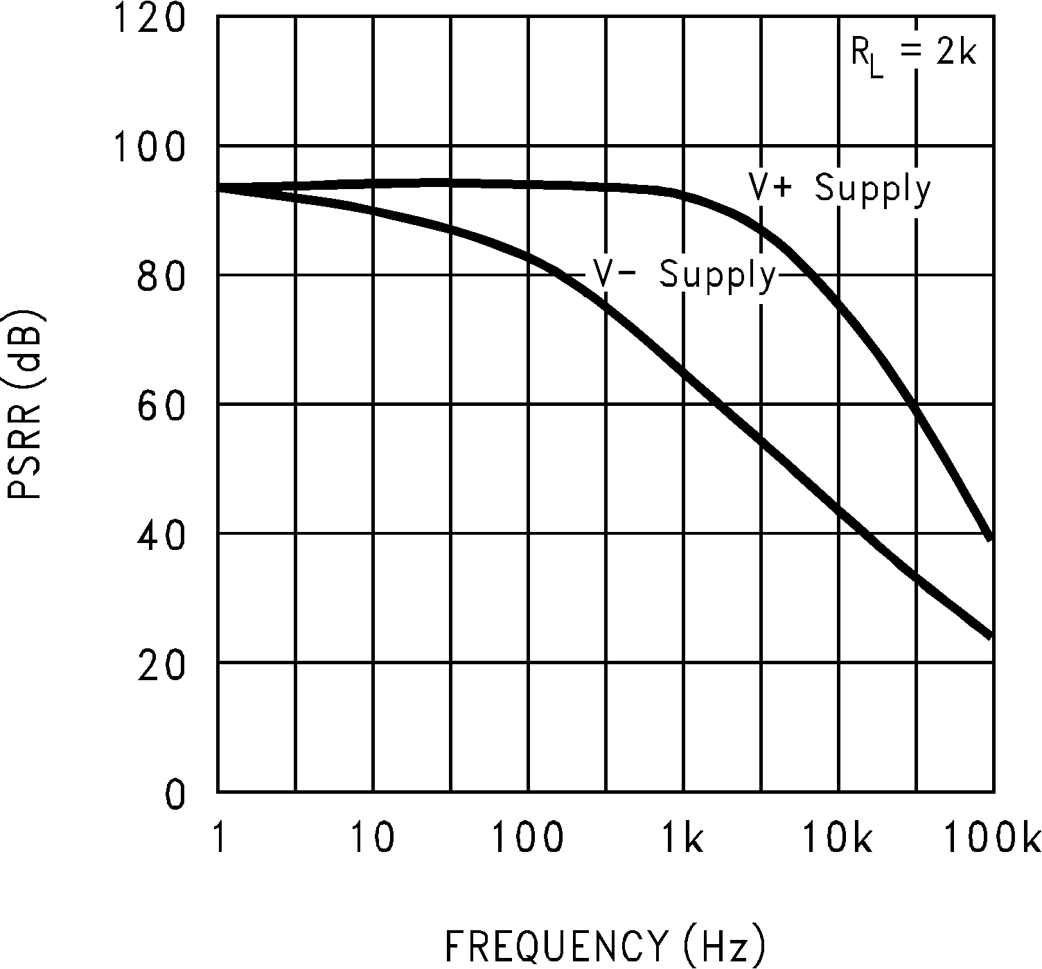
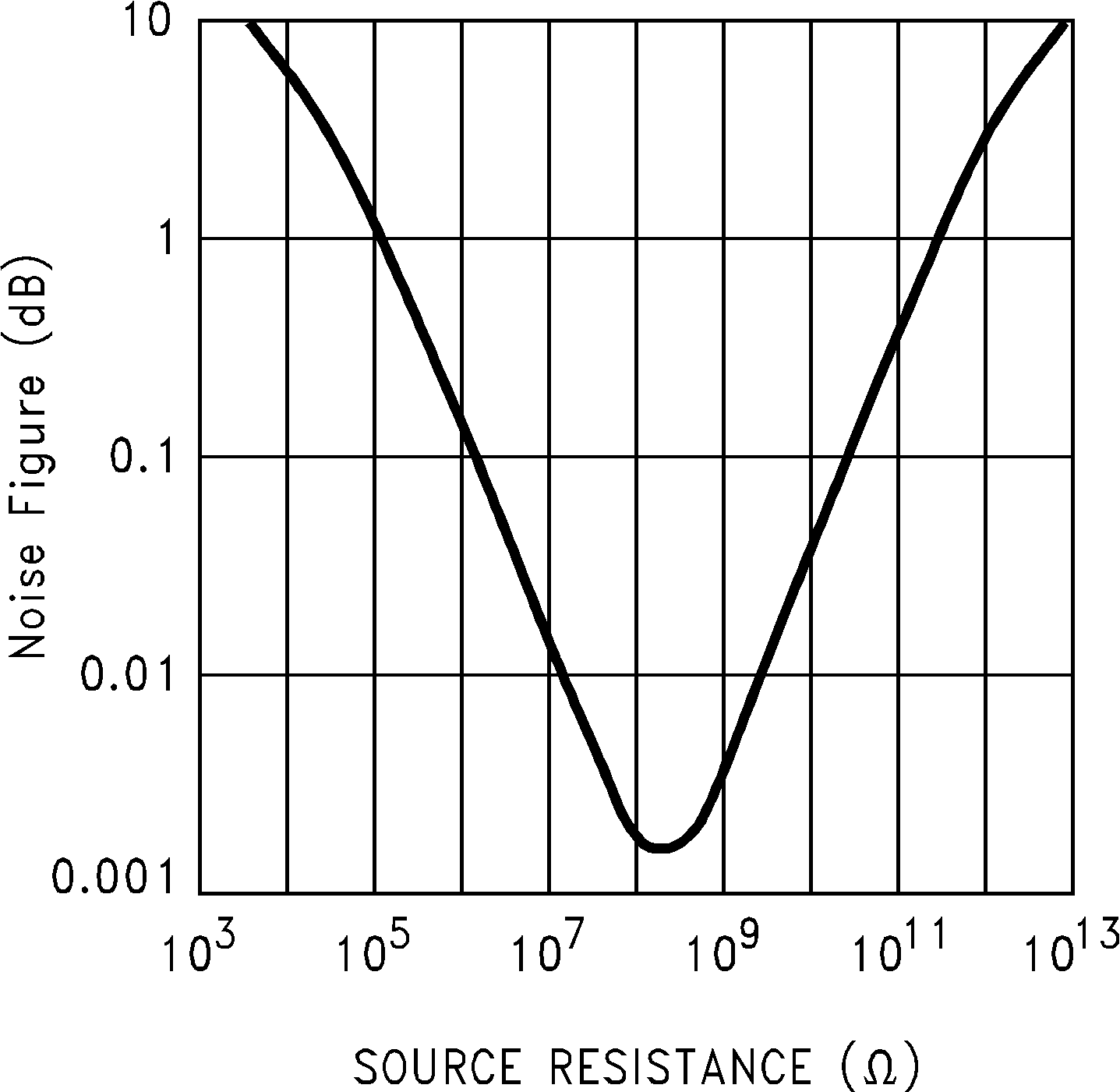
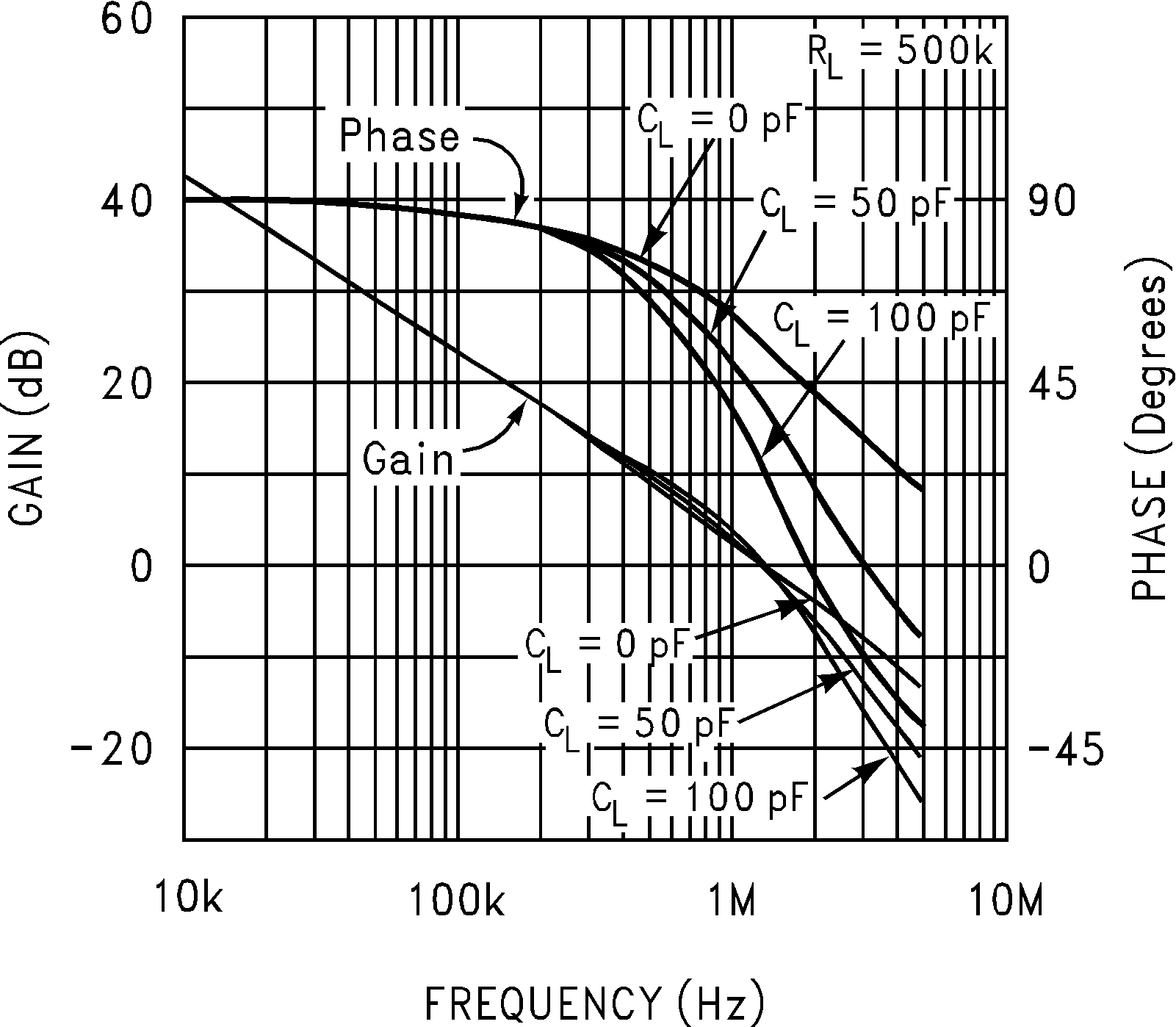
| RL = 500 kω | ||
