SBOS709A July 2016 – July 2016 LMH2832
PRODUCTION DATA.
- 1 Features
- 2 Applications
- 3 Description
- 4 Revision History
- 5 Device Comparison Table
- 6 Pin Configuration and Functions
- 7 Specifications
- 8 Parameter Measurement Information
- 9 Detailed Description
- 10Application and Implementation
- 11Power Supply Recommendations
- 12Layout
- 13Device and Documentation Support
- 14Mechanical, Packaging, and Orderable Information
Package Options
Mechanical Data (Package|Pins)
- RHA|40
Thermal pad, mechanical data (Package|Pins)
- RHA|40
Orderable Information
13 Device and Documentation Support
13.1 Device Support
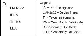
13.1.1 Device Nomenclature
 Figure 64. Device Marking Information
13.2 Documentation Support
13.2.1 Related Documentation
For related documentation see the following:
- ADS54J40 Dual-Channel, 14-Bit, 1.0-GSPS Analog-to-Digital Converter Data Sheet (SBAS714)
- LMH3401 7-GHz, Ultra-Wideband, Fixed-Gain, Fully-Differential Amplifier Data Sheet (SBOS695)
- LMH5401 8-GHz, Low-Noise, Low-Power, Fully-Differential Amplifier Data Sheet (SBOS710)
- LMH6521 High Performance Dual DVGA Data Sheet (SNOSB47)
- LMH3404 Dual-Channel, 7-GHz, Low-Noise, Low-Power, Fully Differential Amplifier Data Sheet (SBOS739)
- LMH3402 Dual, Selectable-Gain, 7-GHz, Low-Noise, Low-Power, Fully Differential Amplifier Data Sheet (SBOS744)
- LMH2832EVM-50 Evaluation Module User's Guide (SLOU454)
- LMH2832EVM-75 Evaluation Module User's Guide (SLOU438)
- LMH2832 TINA-TI Reference Design (SBOMA21)
- LMH2832 TINA-TI Spice Model (SBOMA22)
13.3 Receiving Notification of Documentation Updates
To receive notification of documentation updates, navigate to the device product folder on ti.com. In the upper right corner, click on Alert me to register and receive a weekly digest of any product information that has changed. For change details, review the revision history included in any revised document.
13.4 Community Resources
The following links connect to TI community resources. Linked contents are provided "AS IS" by the respective contributors. They do not constitute TI specifications and do not necessarily reflect TI's views; see TI's Terms of Use.
-
TI E2E™ Online Community TI's Engineer-to-Engineer (E2E) Community. Created to foster collaboration among engineers. At e2e.ti.com, you can ask questions, share knowledge, explore ideas and help solve problems with fellow engineers.
-
Design Support TI's Design Support Quickly find helpful E2E forums along with design support tools and contact information for technical support.
13.5 Trademarks
E2E is a trademark of Texas Instruments.
Keysight Technologies is a trademark of Keysight Technologies.
SPI is a trademark of Motorola Mobility LLC.
All other trademarks are the property of their respective owners.
13.6 Electrostatic Discharge Caution

This integrated circuit can be damaged by ESD. Texas Instruments recommends that all integrated circuits be handled with appropriate precautions. Failure to observe proper handling and installation procedures can cause damage.
ESD damage can range from subtle performance degradation to complete device failure. Precision integrated circuits may be more susceptible to damage because very small parametric changes could cause the device not to meet its published specifications.
13.7 Glossary
SLYZ022 — TI Glossary.
This glossary lists and explains terms, acronyms, and definitions.