SBOS730A April 2015 – May 2015 LMH6401
PRODUCTION DATA.
- 1 Features
- 2 Applications
- 3 Description
- 4 Revision History
- 5 Device Options
- 6 Pin Configuration and Functions
- 7 Specifications
- 8 Parameter Measurement Information
-
9 Detailed Description
- 9.1 Overview
- 9.2 Functional Block Diagram
- 9.3 Feature Description
- 9.4 Device Functional Modes
- 9.5 Programming
- 9.6
Register Maps
- 9.6.1 Revision ID (address = 0h, Read-Only) [default = 03h]
- 9.6.2 Product ID (address = 1h, Read-Only) [default = 00h]
- 9.6.3 Gain Control (address = 2h) [default = 20h]
- 9.6.4 Reserved (address = 3h) [default = 8Ch]
- 9.6.5 Thermal Feedback Gain Control (address = 4h) [default = 27h]
- 9.6.6 Thermal Feedback Frequency Control (address = 5h) [default = 45h]
- 10Application and Implementation
- 11Power-Supply Recommendations
- 12Layout
- 13Device and Documentation Support
- 14Mechanical, Packaging, and Orderable Information
Package Options
Mechanical Data (Package|Pins)
- RMZ|16
Thermal pad, mechanical data (Package|Pins)
Orderable Information
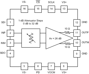
6 Pin Configuration and Functions
RMZ Package
UQFN-16
Top View

Pin Functions
| PIN | FUNCTION | DESCRIPTION | |
|---|---|---|---|
| NO. | NAME | ||
| 1 | SDI | Input | Serial interface input data |
| 2 | INP | Input | Positive input pin |
| 3 | INM | Input | Negative input pin |
| 4 | SDO | Output | Serial interface output data |
| 5 | VS– | Power | Negative supply voltage |
| 6 | PD | Input | Power-down pin. 0 = amplifier enabled, 1 = amplifier disabled |
| 7 | VOCM | Input | Input pin to set amplifier output common-mode voltage |
| 8 | VS+ | Power | Positive supply voltage |
| 9 | GND | Power | Ground |
| 10 | OUTM | Output | Negative output pin |
| 11 | OUTP | Output | Positive output pin |
| 12 | GND | Power | Ground |
| 13 | VS+ | Power | Positive supply voltage |
| 14 | SCLK | Input | Serial interface clock |
| 15 | CS | Input | Chip select |
| 16 | VS– | Power | Negative supply voltage |