SNOSAK9F June 2006 – June 2015 LMH6601 , LMH6601-Q1
PRODUCTION DATA.
- 1 Features
- 2 Applications
- 3 Description
- 4 Revision History
- 5 Pin Configuration and Functions
-
6 Specifications
- 6.1 Absolute Maximum Ratings
- 6.2 ESD Ratings - for LMH6601
- 6.3 ESD Ratings - for LMH6601-Q1
- 6.4 Recommended Operating Conditions
- 6.5 Thermal Information
- 6.6 Electrical Characteristics, 5 V
- 6.7 Electrical Characteristics, 3.3 V
- 6.8 Electrical Characteristics, 2.7 V
- 6.9 Switching Characteristics, 5 V
- 6.10 Switching Characteristics, 3.3 V
- 6.11 Switching Characteristics, 2.7 V
- 6.12 Typical Characteristics
- 7 Detailed Description
- 8 Application and Implementation
- 9 Power Supply Recommendations
- 10Layout
- 11Device and Documentation Support
- 12Mechanical, Packaging, and Orderable Information
Package Options
Mechanical Data (Package|Pins)
- DCK|6
Thermal pad, mechanical data (Package|Pins)
- DCK|6
Orderable Information
1 Features
- LMH6601-Q1 Qualified for Automotive Applications
- AEC-Q100 Grade 3
- –40°C to 85°C Ambient Operating Temperature Range
- VS = 3.3 V, TA = 25°C, AV = 2 V/V, RL = 150 Ω to V−, Unless Specified
- 125 MHz −3 dB Small Signal Bandwidth
- 75 MHz −3 dB Large Signal Bandwidth
- 30 MHz Large Signal 0.1-dB Gain Flatness
- 260 V/μs Slew Rate
- 0.25%/0.25° Differential Gain and Differential Phase
- Rail-to-Rail Output
- 2.4-V to 5.5-V Single-Supply Operating Range
- 6-Pin SC70 Package
2 Applications
- Video Amplifiers
- Charge Amplifiers
- Set-Top Boxes
- Sample and Holds
- Transimpedance Amplifiers
- Line Drivers
- High-Impedance Buffers
- Automotive
3 Description
The LMH6601 device is a low-voltage (2.4 V to 5.5 V), high-speed voltage feedback operational amplifier suitable for use in a variety of consumer and industrial applications. With a bandwidth of 125 MHz at a gain of +2 and ensured high-output current of 100 mA, the LMH6601 is an ideal choice for video line driver applications, including HDTV. Low-input bias current (50 pA maximum), rail-to-rail output, and low current noise allow the use of the LMH6601 in various industrial applications such as transimpedance amplifiers, active filters, or high-impedance buffers. The LMH6601 is an attractive solution for systems which require high performance at low supply voltages. The LMH6601 is available in a 6-pin SC70 package, and includes a micropower shutdown feature.
Device Information(1)
| PART NUMBER | PACKAGE | BODY SIZE (NOM) |
|---|---|---|
| LMH6601 | SC70 (6) | 2.00 mm × 1.25 mm |
| LMH6601-Q1 |
- For all available packages, see the orderable addendum at the end of the data sheet.
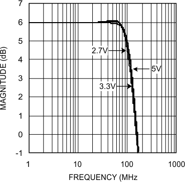
Response at a Gain of +2
for Various Supply Voltages

4 Revision History
Changes from E Revision (March 2013) to F Revision
- Added Pin Configuration and Functions section, ESD Ratings table, Feature Description section, Device Functional Modes, Application and Implementation section, Power Supply Recommendations section, Layout section, Device and Documentation Support section, and Mechanical, Packaging, and Orderable Information section Go
- Removed IOS over temperature limit in Electrical Characteristics, 2.7 VGo
- Moved the SAG Compensation section to the Typical Application section.Go
- Changed section titled Other Applications to Charge PreamplifierGo
Changes from D Revision (March 2013) to E Revision
- Changed layout of National Data Sheet to TI formatGo