SNOSA42G November 2002 – December 2014 LMH6624 , LMH6626
PRODUCTION DATA.
- 1 Features
- 2 Applications
- 3 Description
- 4 Revision History
- 5 Pin Configuration and Functions
- 6 Specifications
- 7 Detailed Description
- 8 Application and Implementation
- 9 Power Supply Recommendations
- 10Layout
- 11Device and Documentation Support
- 12Mechanical, Packaging, and Orderable Information
Package Options
Mechanical Data (Package|Pins)
Thermal pad, mechanical data (Package|Pins)
Orderable Information
10 Layout
10.1 Layout Guidelines
TI suggests the copper patterns on the evaluation boards shown in Figure 62 and Figure 63 as a guide for high frequency layout. These boards are also useful as an aid in device testing and characterization. As is the case with all high-speed amplifiers, accepted-practice RF design technique on the PCB layout is mandatory. Generally, a good high frequency layout exhibits a separation of power supply and ground traces from the inverting input and output pins as shown in Figure 62. Parasitic capacitances between these nodes and ground may cause frequency response peaking and possible circuit oscillations. See Application Note OA-15, Frequent Faux Pas in Applying Wideband Current Feedback Amplifiers (SNOA367) for more information. Use high quality chip capacitors with values in the range of 1000 pF to 0.1 µF for power supply bypassing as shown in Figure 62. One terminal of each chip capacitor is connected to the ground plane and the other terminal is connected to a point that is as close as possible to each supply pin as allowed by the manufacturer’s design rules. In addition, connect a tantalum capacitor with a value between 4.7 μF and 10 μF in parallel with the chip capacitor. Signal lines connecting the feedback and gain resistors should be as short as possible to minimize inductance and microstrip line effect as shown in Figure 63. Place input and output termination resistors as close as possible to the input/output pins. Traces greater than 1 inch in length should be impedance matched to the corresponding load termination.
Symmetry between the positive and negative paths in the layout of differential circuitry should be maintained to minimize the imbalance of amplitude and phase of the differential signal.
Component value selection is another important parameter in working with high speed and high performance amplifiers. Choosing external resistors that are large in value compared to the value of other critical components will affect the closed loop behavior of the stage because of the interaction of these resistors with parasitic capacitances. These parasitic capacitors could either be inherent to the device or be a by-product of the board layout and component placement. Moreover, a large resistor will also add more thermal noise to the signal path. Either way, keeping the resistor values low will diminish this interaction. On the other hand, choosing very low value resistors could load down nodes and will contribute to higher overall power dissipation and high distortion.
| DEVICE | PACKAGE | EVALUATION BOARD PART NUMBER |
|---|---|---|
| LMH6624MF | SOT-23–5 | LMH730216 |
| LMH6624MA | SOIC-8 | LMH730227 |
| LMH6626MA | SOIC-8 | LMH730036 |
| LMH6626MM | VSSOP-8 | LMH730123 |
10.2 Layout Example
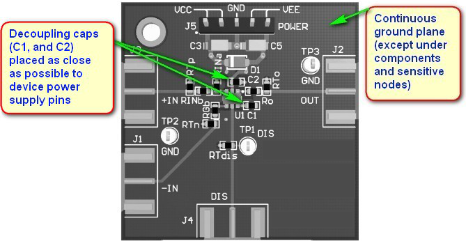 Figure 62. LMH6624 and LMH6626
EVM Board Layout Example
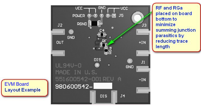 Figure 63. LMH6624 and LMH6626
EVM Board Layout Example