SNOSA42G November 2002 – December 2014 LMH6624 , LMH6626
PRODUCTION DATA.
- 1 Features
- 2 Applications
- 3 Description
- 4 Revision History
- 5 Pin Configuration and Functions
- 6 Specifications
- 7 Detailed Description
- 8 Application and Implementation
- 9 Power Supply Recommendations
- 10Layout
- 11Device and Documentation Support
- 12Mechanical, Packaging, and Orderable Information
Package Options
Mechanical Data (Package|Pins)
Thermal pad, mechanical data (Package|Pins)
Orderable Information
6 Specifications
6.1 Absolute Maximum Ratings
over operating free-air temperature range (unless otherwise noted)(1)| MIN | MAX | UNIT | ||
|---|---|---|---|---|
| VIN Differential | ±1.2 | V | ||
| Supply voltage (V+ - V−) | 13.2 | V | ||
| Voltage at Input pins | V+ +0.5, V− −0.5 |
V | ||
| Input Current | ±10 | mA | ||
| Soldering information | Infrared or convection (20 sec.) | 235 | °C | |
| Wave soldering (10 sec.) | 260 | °C | ||
| Junction temperature(2) | 150 | °C | ||
| Storage temperature | -65 | 150 | °C | |
6.2 ESD Ratings
| VALUE | UNIT | |||
|---|---|---|---|---|
| V(ESD) | Electrostatic discharge | Human-body model (HBM), per ANSI/ESDA/JEDEC JS-001(1) | ±2000 | V |
| Machine model(2) | ±200 | |||
(1) Human body model, 1.5 kΩ in series with 100 pF. JEDEC document JEP155 states that 2000-V HBM allows safe manufacturing with a standard ESD control process. Manufacturing with less than 2000-V HBM is possible with the necessary precautions. Pins listed as ±2000 V may actually have higher performance.
(2) Machine Model, 0 Ω in series with 200 pF. JEDEC document JEP157 states that 200-V MM allows safe manufacturing with a standard ESD control process.
6.3 Recommended Operating Conditions
over operating free-air temperature range (unless otherwise noted)(1)| MIN | MAX | UNIT | |
|---|---|---|---|
| Operating temperature(2) | −40 | +125 | °C |
| Operating supply voltage (V+ - V-) | ±2.25 | ±6.3 | V |
6.4 Thermal Information
| THERMAL METRIC(1) | LMH6624 | LMH6626 | UNIT | |||
|---|---|---|---|---|---|---|
| DBV | D | DGK | D | |||
| 5 PINS | 8 PINS | 8 PINS | 8 PINS | |||
| RθJA | Junction-to-ambient thermal resistance(2) | 265 | 166 | 235 | 166 | °C/W |
(1) For more information about traditional and new thermal metrics, see the IC Package Thermal Metrics application report, SPRA953.
(2) The maximum power dissipation is a function of TJ(MAX), RθJA, and TA. The maximum allowable power dissipation at any ambient temperature is PD = (TJ(MAX) - TA)/ RθJA . All numbers apply for packages soldered directly onto a PC board.
6.5 Electrical Characteristics ±2.5 V
Unless otherwise specified, all limits ensured at TA = 25°C, V+ = 2.5 V, V− = −2.5 V, VCM = 0 V, AV = +20, RF = 500 Ω,RL = 100 Ω. See (9).
| PARAMETER | TEST CONDITIONS | MIN(4) | TYP(3) | MAX(4) | UNIT | ||
|---|---|---|---|---|---|---|---|
| DYNAMIC PERFORMANCE | |||||||
| fCL | −3dB BW | VO = 400 mVPP (LMH6624) | 90 | MHz | |||
| VO = 400 mVPP (LMH6626) | 80 | ||||||
| SR | Slew rate(6) | VO = 2 VPP, AV = +20 (LMH6624) | 300 | V/μs | |||
| VO = 2 VPP, AV = +20 (LMH6626) | 290 | ||||||
| VO = 2 VPP, AV = +10 (LMH6624) | 360 | ||||||
| VO = 2 VPP, AV = +10 (LMH6626) | 340 | ||||||
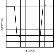
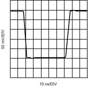
| tr | Rise time | VO = 400 mV Step, 10% to 90% | 4.1 | ns | |||
| tf | Fall time | VO = 400 mV Step, 10% to 90% | 4.1 | ns | |||
| ts | Settling time 0.1% | VO = 2 VPP (Step) | 20 | ns | |||
| DISTORTION and NOISE RESPONSE | |||||||
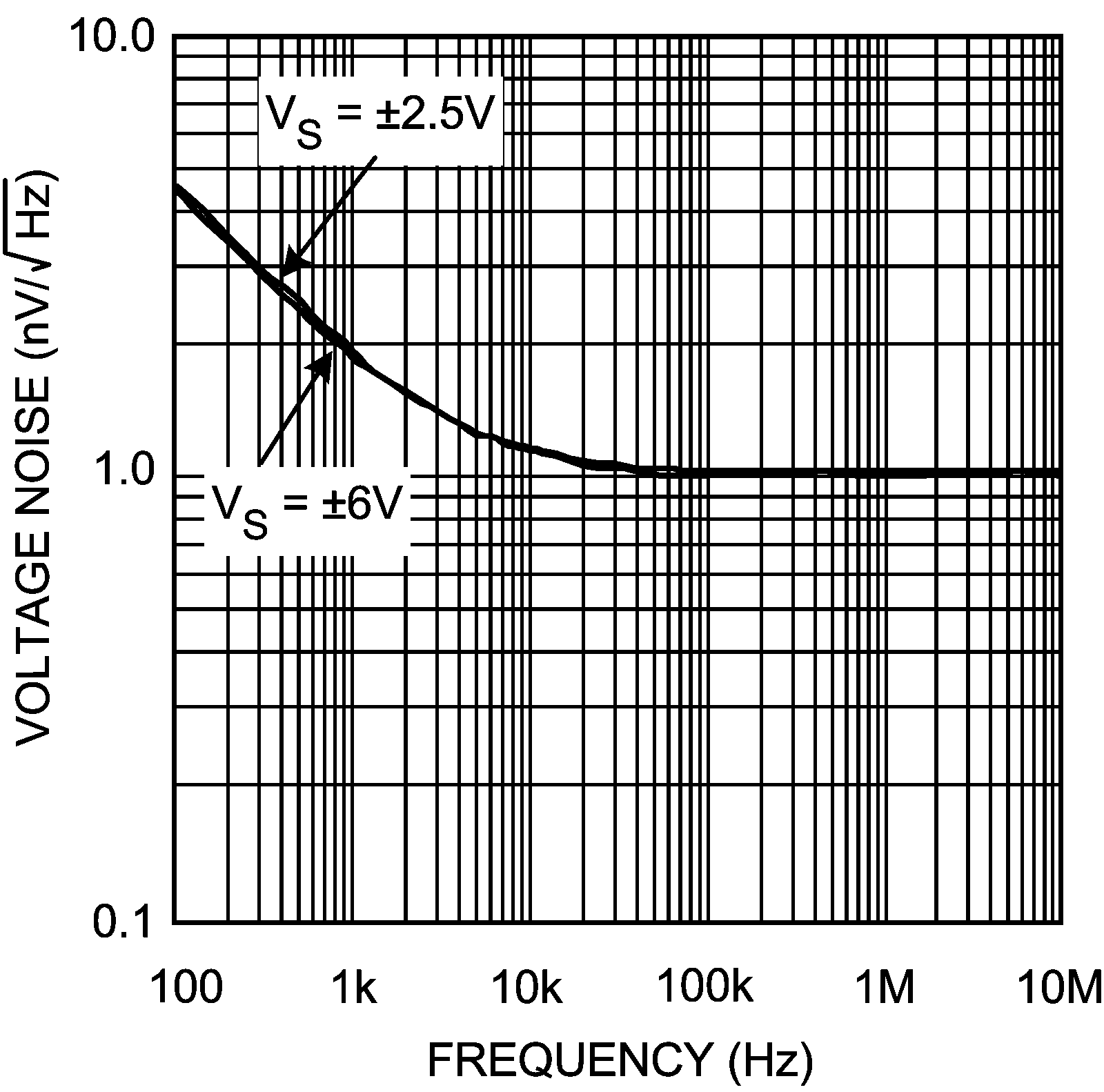
| en | Input referred voltage noise | f = 1 MHz (LMH6624) | 0.92 | nV/√Hz | |||
| f = 1 MHz (LMH6626) | 1.0 | ||||||
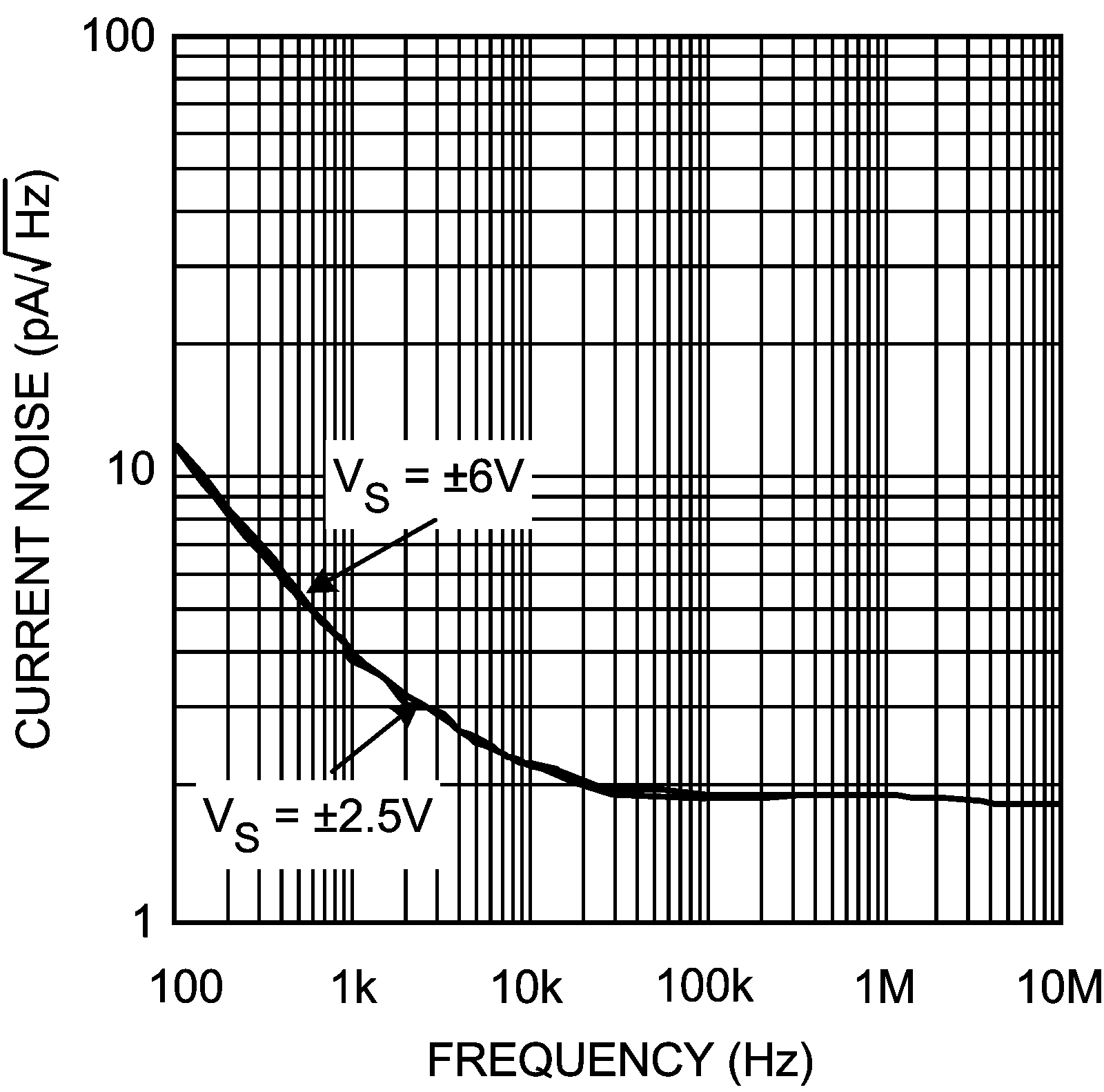
| in | Input referred current noise | f = 1 MHz (LMH6624) | 2.3 | pA/√Hz | |||
| f = 1 MHz (LMH6626) | 1.8 | ||||||
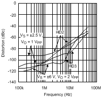
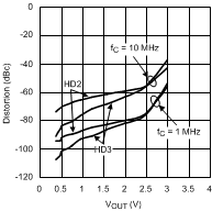
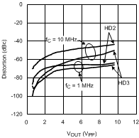
| HD2 | 2nd harmonic distortion | fC = 10 MHz, VO = 1 VPP, RL 100 Ω | −60 | dBc | |||
| HD3 | 3rd harmonic distortion | fC = 10 MHz, VO = 1 VPP, RL 100 Ω | −76 | dBc | |||
| INPUT CHARACTERISTICS | |||||||
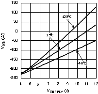
| VOS | Input offset voltage | VCM = 0 V | −0.75 | −0.25 | +0.75 | mV | |
| -40°C ≤ TJ ≤ 125°C | −0.95 | +0.95 | |||||
| Average drift(5) | VCM = 0 V | ±0.25 | μV/°C | ||||
| IOS | Input offset current | VCM = 0 V | −1.5 | −0.05 | +1.5 | μA | |
| -40°C ≤ TJ ≤ 125°C | −2.0 | +2.0 | |||||
| Average drift(5) | VCM = 0 V | 2 | nA/°C | ||||
| IB | Input bias current | VCM = 0 V | 13 | +20 | μA | ||
| -40°C ≤ TJ ≤ 125°C | +25 | ||||||
| Average drift(5) | VCM = 0 V | 12 | nA/°C | ||||
| RIN | Input resistance(7) | Common Mode | 6.6 | MΩ | |||
| Differential Mode | 4.6 | kΩ | |||||
| CIN | Input capacitance(7) | Common Mode | 0.9 | pF | |||
| Differential Mode | 2.0 | ||||||
| CMRR | Common mode rejection ratio | Input Referred, VCM = −0.5 to +1.9 V | 87 | 90 | dB | ||
| Input Referred, VCM = −0.5 to +1.75 V |
-40°C ≤ TJ ≤ 125°C | 85 | |||||
| TRANSFER CHARACTERISTICS | |||||||
| AVOL | Large signal voltage gain | (LMH6624) RL = 100 Ω, VO = −1 V to +1 V |
75 | 79 | dB | ||
| -40°C ≤ TJ ≤ 125°C | 70 | ||||||
| (LMH6626) RL = 100 Ω, VO = −1 V to +1 V |
72 | 79 | |||||
| -40°C ≤ TJ ≤ 125°C | 67 | ||||||
| Xt | Crosstalk rejection | f = 1 MHz (LMH6626) | −75 | dB | |||
| OUTPUT CHARACTERISTICS | |||||||
| VO | Output swing | RL = 100 Ω | ±1.1 | ±1.5 | V | ||
| -40°C ≤ TJ ≤ 125°C | ±1.0 | ||||||
| No Load | ±1.4 | ±1.7 | |||||
| -40°C ≤ TJ ≤ 125°C | ±1.25 | ||||||
| RO | Output impedance | f ≤ 100 KHz | 10 | mΩ | |||
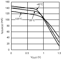
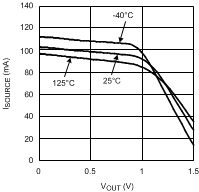
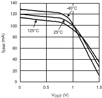
| ISC | Output short circuit current | (LMH6624) Sourcing to Ground ΔVIN = 200 mV (2)(8) |
90 | 145 | mA | ||
| -40°C ≤ TJ ≤ 125°C | 75 | ||||||
| (LMH6624) Sinking to Ground ΔVIN = −200 mV (2)(8) |
90 | 145 | |||||
| -40°C ≤ TJ ≤ 125°C | 75 | ||||||
| (LMH6626) Sourcing to Ground ΔVIN = 200 mV (2)(8) |
60 | 120 | |||||
| -40°C ≤ TJ ≤ 125°C | 50 | ||||||
| (LMH6626) Sinking to Ground ΔVIN = −200 mV (2)(8) |
60 | 120 | |||||
| -40°C ≤ TJ ≤ 125°C | 50 | ||||||
| IOUT | Output current | (LMH6624) Sourcing, VO = +0.8 V Sinking, VO = −0.8 V |
100 | mA | |||
| (LMH6626) Sourcing, VO = +0.8 V Sinking, VO = −0.8 V |
75 | ||||||
| POWER SUPPLY | |||||||
| PSRR | Power supply rejection ratio | VS = ±2.0 V to ±3.0 V | 82 |
90 | dB | ||
| -40°C ≤ TJ ≤ 125°C | 80 | ||||||
| IS | Supply current (per channel) | No Load | 11.4 | 16 | mA | ||
| -40°C ≤ TJ ≤ 125°C | 18 | ||||||
6.6 Electrical Characteristics ±6 V
Unless otherwise specified, all limits ensured at TA = 25°C, V+ = 6 V, V− = −6 V, VCM = 0 V, AV = +20, RF = 500 Ω,RL = 100 Ω. See (9).
| PARAMETER | TEST CONDITIONS | MIN(4) | TYP(3) | MAX(4) | UNIT | ||
|---|---|---|---|---|---|---|---|
| DYNAMIC PERFORMANCE | |||||||
| fCL | −3dB BW | VO = 400 mVPP (LMH6624) | 95 | MHz | |||
| VO = 400 mVPP (LMH6626) | 85 | ||||||
| SR | Slew rate(6) | VO = 2 VPP, AV = +20 (LMH6624) | 350 | V/μs | |||
| VO = 2 VPP, AV = +20 (LMH6626) | 320 | ||||||
| VO = 2 VPP, AV = +10 (LMH6624) | 400 | ||||||
| VO = 2 VPP, AV = +10 (LMH6626) | 360 | ||||||
| tr | Rise time | VO = 400 mV Step, 10% to 90% | 3.7 | ns | |||
| tf | Fall time | VO = 400 mV Step, 10% to 90% | 3.7 | ns | |||
| ts | Settling time 0.1% | VO = 2 VPP (Step) | 18 | ns | |||
| DISTORTION and NOISE RESPONSE | |||||||
| en | Input referred voltage noise | f = 1 MHz (LMH6624) | 0.92 | nV/√Hz | |||
| f = 1 MHz (LMH6626) | 1.0 | ||||||
| in | Input referred current noise | f = 1 MHz (LMH6624) | 2.3 | pA/√Hz | |||
| f = 1 MHz (LMH6626) | 1.8 | ||||||
| HD2 | 2nd harmonic distortion | fC = 10 MHz, VO = 1 VPP, RL = 100 Ω | −63 | dBc | |||
| HD3 | 3rd harmonic distortion | fC = 10 MHz, VO = 1 VPP, RL = 100 Ω | −80 | dBc | |||
| INPUT CHARACTERISTICS | |||||||
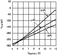
| VOS | Input offset voltage | VCM = 0 V | −0.5 | ±0.10 | +0.5 | mV | |
| -40°C ≤ TJ ≤ 125°C | −0.7 | +0.7 | |||||
| Average drift(5) | VCM = 0 V | ±0.2 | μV/°C | ||||
| IOS | Input offset current | (LMH6624) VCM = 0 V |
−1.1 |
0.05 | 1.1 | μA | |
| -40°C ≤ TJ ≤ 125°C | −2.5 | 2.5 | |||||
| (LMH6626) VCM = 0 V |
−2.0 | 0.1 | 2.0 | ||||
| -40°C ≤ TJ ≤ 125°C | −2.5 | 2.5 | |||||
| Average drift(5) | VCM = 0 V | 0.7 | nA/°C | ||||
| IB | Input bias current | VCM = 0 V | 13 | +20 | μA | ||
| -40°C ≤ TJ ≤ 125°C | +25 | ||||||
| Average drift(5) | VCM = 0 V | 12 | nA/°C | ||||
| RIN | Input resistance(7) | Common Mode | 6.6 | MΩ | |||
| Differential Mode | 4.6 | kΩ | |||||
| CIN | Input capacitance(7) | Common Mode | 0.9 | pF | |||
| Differential Mode | 2.0 | ||||||
| CMRR | Common mode rejection ratio | Input Referred, VCM = −4.5 to +5.25 V | 90 | 95 | dB | ||
| Input Referred, VCM = −4.5 to +5.0 V |
-40°C ≤ TJ ≤ 125°C | 87 | |||||
| TRANSFER CHARACTERISTICS | |||||||
| AVOL | Large signal voltage gain | (LMH6624) RL = 100 Ω, VO = −3 V to +3 V |
77 |
81 | dB | ||
| -40°C ≤ TJ ≤ 125°C | 72 | ||||||
| (LMH6626) RL = 100 Ω, VO = −3 V to +3 V |
74 | 80 | |||||
| -40°C ≤ TJ ≤ 125°C | 70 | ||||||
| Xt | Crosstalk rejection | f = 1MHz (LMH6626) | −75 | dB | |||
| OUTPUT CHARACTERISTICS | |||||||
| VO | Output swing | (LMH6624) RL = 100 Ω |
±4.4 | ±4.9 | V | ||
| -40°C ≤ TJ ≤ 125°C | ±4.3 | ||||||
| (LMH6624) No Load |
±4.8 | ±5.2 | |||||
| -40°C ≤ TJ ≤ 125°C | ±4.65 | ||||||
| (LMH6626) RL = 100 Ω |
±4.3 | ±4.8 | |||||
| -40°C ≤ TJ ≤ 125°C | ±4.2 | ||||||
| (LMH6626) No Load |
±4.8 | ±5.2 | |||||
| -40°C ≤ TJ ≤ 125°C | ±4.65 | ||||||
| RO | Output impedance | f ≤ 100 KHz | 10 | mΩ | |||
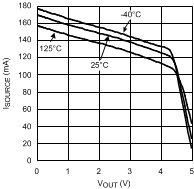
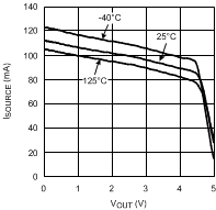
| ISC | Output short circuit current | (LMH6624) Sourcing to Ground ΔVIN = 200 mV (2)(8) |
100 | 156 | mA | ||
| -40°C ≤ TJ ≤ 125°C | 85 | ||||||
| (LMH6624) Sinking to Ground ΔVIN = −200 mV (2)(8) |
100 | 156 | |||||
| -40°C ≤ TJ ≤ 125°C | 85 | ||||||
| (LMH6626) Sourcing to Ground ΔVIN = 200 mV (2)(8) |
65 | 120 | |||||
| -40°C ≤ TJ ≤ 125°C | 55 | ||||||
| (LMH6626) Sinking to Ground ΔVIN = −200 mV(2)(8) |
65 | 120 | |||||
| -40°C ≤ TJ ≤ 125°C | 55 | ||||||
| IOUT | Output current | (LMH6624) Sourcing, VO = +4.3 V Sinking, VO = −4.3 V |
100 | mA | |||
| (LMH6626) Sourcing, VO = +4.3 V Sinking, VO = −4.3 V |
80 | ||||||
| POWER SUPPLY | |||||||
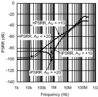
| PSRR | Power supply rejection ratio | VS = ±5.4 V to ±6.6 V | 82 | 88 | dB | ||
| -40°C ≤ TJ ≤ 125°C | 80 | ||||||
| IS | Supply current (per channel) | No Load | 12 | 16 | mA | ||
| -40°C ≤ TJ ≤ 125°C | 18 | ||||||
(1) Absolute maximum ratings indicate limits beyond which damage to the device may occur. Operating Ratings indicate conditions for which the device is intended to be functional, but specific performance is not ensured. For ensured specifications and the test conditions, see the Electrical Characteristics.
(2) Applies to both single-supply and split-supply operation. Continuous short circuit operation at elevated ambient temperature can result in exceeding the maximum allowed junction temperature of 150°C.
(3) Typical Values represent the most likely parametric norm.
(4) All limits are specified by testing or statistical analysis.
(5) Average drift is determined by dividing the change in parameter at temperature extremes into the total temperature change.
(6) Slew rate is the slowest of the rising and falling slew rates.
(7) Simulation results.
(8) Short circuit test is a momentary test. Output short circuit duration is 1.5 ms.
(9) Electrical table values apply only for factory testing conditions at the temperature indicated. Factory testing conditions result in very limited self-heating of the device such that TJ = TA. No ensured specification of parametric performance is indicated in the electrical tables under conditions of internal self-heating where TJ > TA. Absolute maximum ratings indicate junction temperature limits beyond which the device may be permanently degraded, either mechanically or electrically.
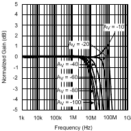
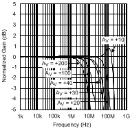
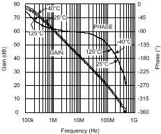
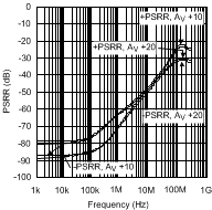
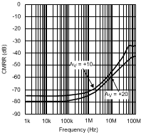
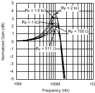
6.7 Typical Characteristics
| VS = ±2.5 V | ||
| VIN = 5 mVpp | ||
| RL = 100 Ω |
| VS = ±2.5 V | ||
| RF = 500 Ω | ||
| VO = 2 Vpp |
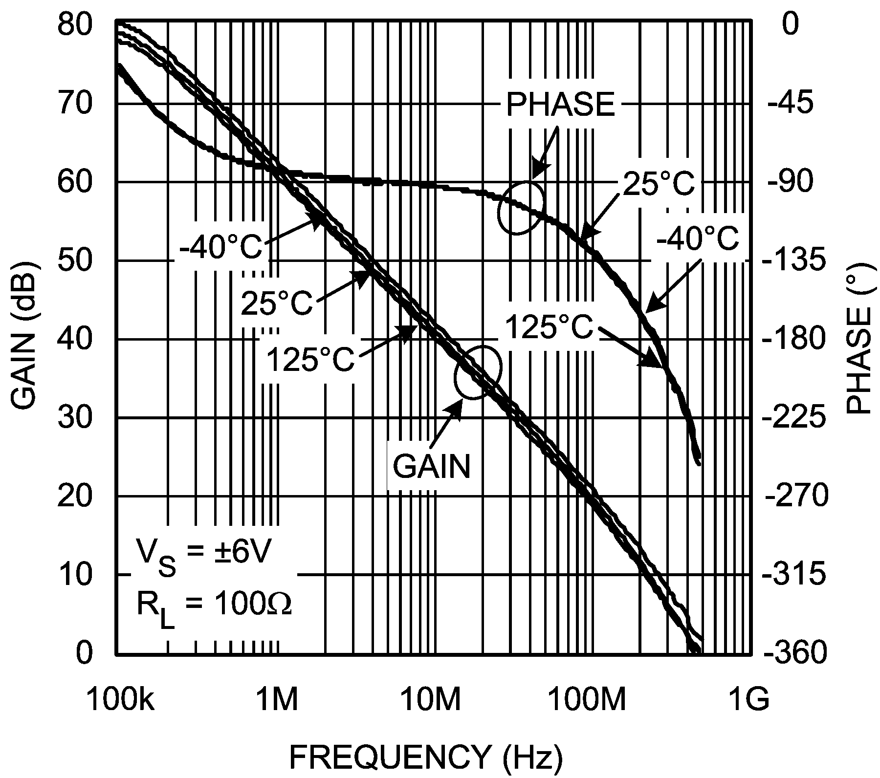
| VS = ±2.5 V | ||
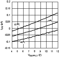
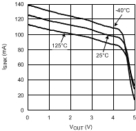
Over Temperature
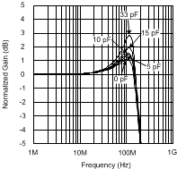
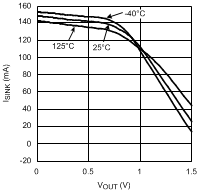
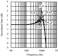
| VS = ±2.5V | RISO = 10 Ω | |
| AV = +10 | RL = 1 kΩ||CL | |
| RF = 250 Ω |
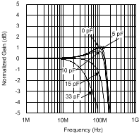
| VS = ±2.5 V | RISO = 100 Ω | |
| AV = +10 | RL = 1 kΩ||CL | |
| RF = 250 Ω |
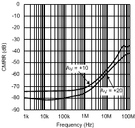
| VS = ±-2.5 V | ||
| AV = +10 | ||
| RF = 500 Ω |
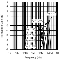
| VS = ±2.5 V | ||
| AV = +20 | ||
| RF = 500 Ω |
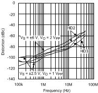
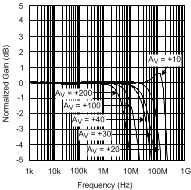
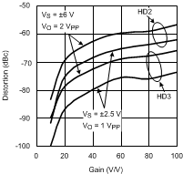
| VS = ±6 V | ||
| AV = +20 | ||
| RF = 500 Ω |
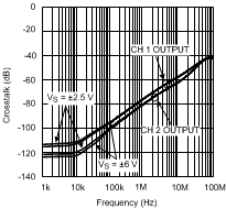
| VS = ±2.5 V | ||
| VS = ±6 V | ||
| VS = ±2.5 V | ||
| VS = ±6 V | ||
| AV = +10 | ||
| RL = 100 Ω | ||
| AV = +20 | ||
| RL = 500 Ω | ||
| AV = +20 | ||
| AV = ±2.5V | ||
| RL = 100 Ω |
| VS = ±2.5 V | RL = 100 Ω | |
| VO = 1 Vpp | ||
| AV = +10 |
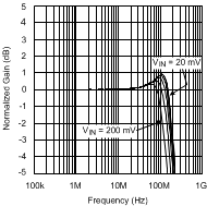
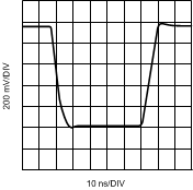
| VS = ±2.5 V | RL = 100 Ω | |
| VO = 200 mv | ||
| AV = +10 |
| VS = ±2.5 V | ||
| VS = ±2.5V | ||
| VIN = 5 mVpp | ||
| VS = ±2.5 V | ||
| AV = +10 | ||
| RL = 100 Ω |
| VS = ±6V | ||
| VIN = 5 mVpp | ||
| RL = 100 Ω |
| VS = ±6 V | ||
| RF = 500 Ω | ||
| VO = 2 Vpp |
| VS = ±6V | ||
| RL = 100 Ω | ||
Over Temperature
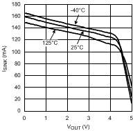
| VS = ±6V | RISO = 10 Ω | |
| AV = +10 | RL = 1 kΩ||CL | |
| RF = 250 Ω |
| VS = ±6 V | RISO = 10 Ω | |
| AV = +10 | RL = 1 kΩ||CL | |
| RF = 250 Ω |
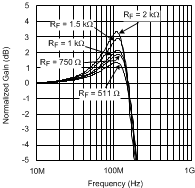
| VS = ±6 V | ||
| AV = +10 | ||
| RF = 500 Ω |
| VS = ±2.5 V | ||
| AV = +20 | ||
| RF = 500 Ω |
| VS = ±6 V | ||
| AV = +20 | ||
| RF = 500 Ω |
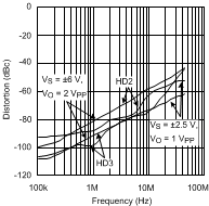
| VS = ±2.5 V | ||
| VS = ±6 V | ||
| VS = ±2.5V | ||
| VS = ±6 V | ||
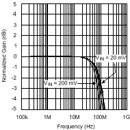
| VIN = 60 mVpp | ||
| AV = +20 | ||
| RL = 100 Ω |
| AV = +20 | ||
| RL = 100 Ω | ||
| VS = ±6 V | ||
| VO = 2 Vpp | ||
| AV = +20 | ||
| VS = ±6 V | ||
| RL = 100 Ω |
| VS = ±6 V | RL = 100 Ω | |
| VO = 1 Vpp | ||
| AV = +20 |
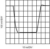
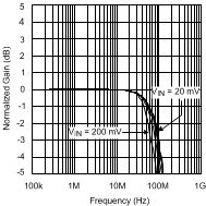
| VS = ±6 V | RL = 100 Ω | |
| VO = 500 mv | ||
| AV = +20 |
| VS = ±6 V | ||
| VS = ±6 V | ||
| VIN = 5 mVpp | ||
| VS = ±6 V | ||
| AV = +10 V | ||
| RL = 100 Ω |