SNOSB18I April 2010 – December 2014 LMH6629
PRODUCTION DATA.
- 1 Features
- 2 Applications
- 3 Description
- 4 Revision History
- 5 Pin Configuration and Functions
- 6 Specifications
-
7 Detailed Description
- 7.1 Overview
- 7.2 Functional Block Diagram
- 7.3
Feature Description
- 7.3.1 WSON-8 Control Pins and SOT-23-5 Comparison
- 7.3.2 Compensation
- 7.3.3 Cancellation of Offset Errors Due to Input Bias Currents
- 7.3.4 Total Input Noise vs. Source Resistance
- 7.3.5 Noise Figure
- 7.3.6 Single-Supply Operation
- 7.3.7 Low-Noise Transimpedance Amplifier
- 7.3.8 Low-Noise Integrator
- 7.3.9 High-Gain Sallen-Key Active Filters
- 7.4 Device Functional Modes
- 8 Application and Implementation
- 9 Power Supply Recommendations
- 10Layout
- 11Device and Documentation Support
- 12Mechanical, Packaging, and Orderable Information
Package Options
Mechanical Data (Package|Pins)
Thermal pad, mechanical data (Package|Pins)
Orderable Information
7 Detailed Description
7.1 Overview
The LMH6629 is a high gain bandwidth, ultra low-noise voltage feedback operational amplifier. The excellent noise and bandwidth enables applications such as medical diagnostic ultrasound, magnetic tape and disk storage and fiberoptics to achieve maximum high frequency signal-to-noise ratios. The following discussion will enable the proper selection of external components to achieve optimum system performance.
7.2 Functional Block Diagram
The LMH6629 (WSON-8 package only) has some additional features to allow maximum flexibility. As shown in Figure 48, there are provisions for low-power shutdown and two internal compensation settings, which are discussed in more detail in Compensation. Also provided is a feedback (FB) pin which allows the placement of the feedback resistor directly adjacent to the inverting input (IN-) pin. This pin simplifies printed circuit board layout and minimizes the possibility of unwanted interaction between the feedback path and other circuit elements.
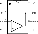 Figure 48. 8-Pin WSON Pinout Diagram
The WSON-8 package requires the bottom-side Die Attach Paddle (DAP) to be soldered to the circuit board for proper thermal dissipation and to get the thermal resistance number specified. The DAP is tied to the V- potential within the LMH6629 package. Thus, the circuit board copper area devoted to DAP heatsinking connection should be at the V- potential as well. Please refer to the package drawing for the recommended land pattern and recommended DAP connection dimensions.
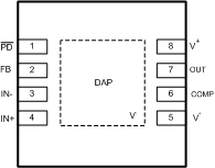 Figure 49. WSON–8 DAP(Top View)
7.3 Feature Description
7.3.1 WSON-8 Control Pins and SOT-23-5 Comparison
The LMH6629 WSON-8 package has two digital control pins; PD and COMP pins. The PD pin, used for power down, floats high (device on) when not driven. When the PD pin is pulled low, the amplifier is disabled and the amplifier output stage goes into a high impedance state so the feedback and gain set resistors determine the output impedance of the circuit. The other control pin, the COMP pin, allows control of the internal compensation and defaults to the lower gain mode or logic 0.
The SOT-23-5 package has the following differences relative to the WSON-8 package:
- No power down (shutdown) capability.
- No COMP pin to set the minimum stable gain. SOT-23–5 package minimum stable gain is internally fixed to be 10V/V.
- No feedback (FB) pin.
From a performance point of view, the WSON-8 and the SOT-23-5 packages perform very similarly except in the following areas:
- SSBW, Peaking, and 0.1 dB Bandwidth: These differences are highlighted in the Typical Performance Characteristics and the Electrical Characteristics 5V tables. Most notable differences are with small signal (0.2 Vpp) and close to the minimum stable gain of 10V/V.
- Distortion: It is possible to get slightly different distortion performance. The board layout and decoupling capacitor return current routing strongly influence distortion performance.
- Output Current: In heavy current applications, there will be differences between these package types because of the difference in their respective Thermal Resistances (RθJA).
7.3.2 Compensation
The LMH6629 has two compensation settings that can be controlled by the COMP pin (WSON-8 package only). The default setting is set through an internal pulldown resistor and places the COMP pin at the logic 0 state. In this configuration the on-chip compensation is set to the maximum and bandwidth is reduced to enable stability at gains as low as 4V/V.
When this pin is driven to the logic 1 state, the internal compensation is decreased to allow higher bandwidth at higher gains. In this state, the minimum stable gain is 10V/V. Due to the reduced compensation, slew rate and large signal bandwidth are significantly enhanced for the higher gains.
NOTE
As mentioned earlier, the SOT-23-5 package does not offer the two compensation settings that the WSON-8 offers. The SOT-23-5 is internally set for a minimum gain of 10 V/V.
It is possible to externally compensate the LMH6629 for any of the following reasons, as shown in Figure 50.
- To operate the SOT-23-5 package (which does not offer the COMP pin) at closed loop gains < 10V/V.
- To operate the WSON-8 package at gains below the minimum stable gain of 4V /V when the COMP pin is LO. NOTE: In this case, Figure 50 “Constraint 1” may be changed to ≥ 4 V/V instead of ≥ 10 V/V.
- To operate either package at low gain and need maximum slew rate (COMP pin HI).
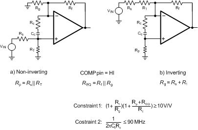 Figure 50. External Compensation
This circuit operates by increasing the Noise Gain (NG) beyond the minimum stable gain of the LMH6629 while maintaining a positive loop gain phase angle at 0 dB. There are two constraints shown in Figure 50: “Constraint 1” ensures that NG has increased to at least 10 V/V when the loop gain approaches 0dB, and “Constraint 2” places an upper limit on the feedback phase lead network frequency to make sure it is fully effective in the frequency range when loop gain approaches 0dB. These two constraints allow one to estimate the “starting value” for Rc and Cc which may need to be fine tuned for proper response.
Here is an example worked out for more clarification:
- Assume that the objective is to use the SOT-23-5 version of the LMH6629 for a closed loop gain of +3.7 V/V using the technique shown in Figure 50.
- Selecting Rf = 249 Ω → Rg = 91 Ω → REQ= 66.6 Ω.
- For 50-Ω source termination (Rs= 50 Ω), select RT= 50 Ω → Rp = 25 Ω.
- Using “Constraint 1” (= 10V/V) allows one to compute Rc ≊ 56 Ω. Using “Constraint 2” (= 90 MHz) defines the appropriate value of Cc ≊ 33 pF.
- The frequency response plot shown in Figure 51 is the measured response with Rc and Cc values computed above and shows a -3 dB response of about 1 GHz.
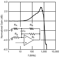
| Cf = 1.5 pF | ||
| RA = 33 Ω | ||
| RB = 91 Ω |
with External Compensation
For the Figure 51 measured results, a compensation capacitor (Cf') was used across Rf to compensate for the summing node net capacitance due to the board and the SOT-23–5 LMH6629. The RA and RB combination reduces the effective capacitance of Cf‘ by the ratio of 1+RB / RA, with the constraint that RB << Rf, thereby allowing a practical capacitance value (> 1pF) to be used. The WSON-8 package does not need this compensation across Rf due to its lower parasitics.
With the COMP pin HI (WSON-8 package only) or with the SOT-23–5 package, this circuit achieves high slew rate and takes advantage of the LMH6629’s superior low-noise characteristics without sacrificing stability, while enabling lower gain applications. It should be noted that the Rc, Cc combination does lower the input impedance and increases noise gain at higher frequencies. With these values, the input impedance reduces by 3 dB at 490 MHz. The Noise Gain transfer function “zero” is given by Equation 1 and it has a 3-dB increase at 32.8 MHz with these values:
External Compensation Noise Gain Increase:
7.3.3 Cancellation of Offset Errors Due to Input Bias Currents
The LMH6629 offers exceptional offset voltage accuracy. In order to preserve the low offset voltage errors, care must be taken to avoid voltage errors due to input bias currents. This is important in both inverting and non-inverting applications.
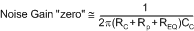
The non-inverting circuit is used here as an example. To cancel the bias current errors of the non-inverting configuration, the parallel combination of the gain setting (Rg) and feedback (Rf) resistors should equal the equivalent source resistance (Rseq) as defined in Figure 52. Combining this constraint with the non-inverting gain equation also seen in Figure 52 allows both Rf and Rg to be determined explicitly from Equation 2:
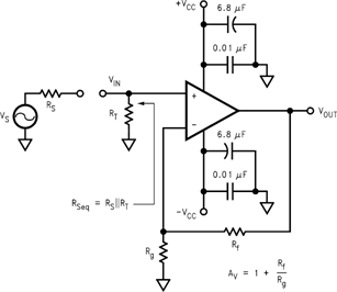 Figure 52. Non-Inverting Amplifier Configuration
When driven from a 0-Ω source, such as the output of an op amp, the non-inverting input of the LMH6629 should be isolated with at least a 25-Ω series resistor.
As seen in Figure 53, bias current cancellation is accomplished for the inverting configuration by placing a resistor (Rb) on the non-inverting input equal in value to the resistance seen by the inverting input (Rf || (Rg+Rs)). Rb should to be no less than 25 Ω for optimum LMH6629 performance. A shunt capacitor (not shown) can minimize the additional noise of Rb.
 Figure 53. Inverting Amplifier Configuration
7.3.4 Total Input Noise vs. Source Resistance
To determine maximum signal-to-noise ratios from the LMH6629, an understanding of the interaction between the amplifier’s intrinsic noise sources and the noise arising from its external resistors is necessary. Figure 54 describes the noise model for the non-inverting amplifier configuration showing all noise sources. In addition to the intrinsic input voltage noise (en) and current noise (in = in+ = in−) source, there is also thermal voltage noise (et = √(4KTR)) associated with each of the external resistors.
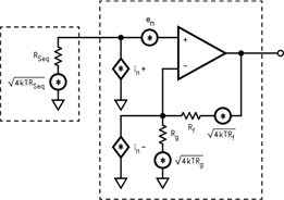 Figure 54. Non-Inverting Amplifier Noise Model
Equation 3 provides the general form for total equivalent input voltage noise density (eni).
General Noise Equation:

Equation 4 is a simplification of Equation 3 that assumes Rf || Rg = Rseq for bias current cancellation:
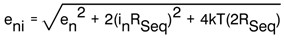
Figure 55 schematically shows eni alongside VIN (the portion of VS source which reaches the non-inverting input of Figure 52) and external components affecting gain (Av= 1 + Rf / Rg), all connected to an ideal noiseless amplifier.
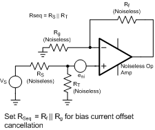 Figure 55. Non-Inverting Amplifier Equivalent Noise Source Schematic
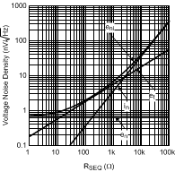
Figure 56 illustrates the equivalent noise model using this assumption. Figure 57 is a plot of eni against equivalent source resistance (Rseq) with all of the contributing voltage noise source of Equation 4. This plot gives the expected eni for a given (Rseq) which assumes Rf||Rg = Rseq for bias current cancellation. The total equivalent output voltage noise (eno) is eni*AV.
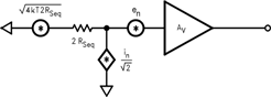 Figure 56. Noise Model with Rf||Rg = Rseq
As seen in Figure 57, eni is dominated by the intrinsic voltage noise (en) of the amplifier for equivalent source resistances below 15 Ω. Between 15 Ω and 2.5 kΩ, eni is dominated by the thermal noise (et = √(4kT(2Rseq)) of the equivalent source resistance Rseq. Incidentally, this is the range of Rseq values where the LMH6629 has the best (lowest) Noise Figure (NF) for the case where Rseq = Rf || Rg.
Above 2.5 kΩ, eni is dominated by the amplifier’s current noise (in = √2 * inRseq). When Rseq = 190 Ω (that is, Rseq = en/√2 * in), the contribution from voltage noise and current noise of LMH6629 is equal. For example, configured with a gain of +10V/V giving a −3dB of 825 MHz and driven from Rseq = Rf || Rg = 20 Ω (eni = 1.07 nV√Hz from Figure 57), the LMH6629 produces a total equivalent output noise voltage (eni * 10 V/V * √(1.57 * 825 MHz)) of 385 μVrms.
| RSEQ = RF || RG | ||
If bias current cancellation is not a requirement, then Rf || Rg does not need to equal Rseq. In this case, according to Equation 3, Rf || Rg should be as low as possible to minimize noise. Results similar to Equation 3 are obtained for the inverting configuration of Figure 53 if Rseq is replaced by Rb and Rg is replaced by Rg + Rs. With these substitutions, Equation 3 will yield an eni referred to the non-inverting input. Referring eni to the inverting input is easily accomplished by multiplying eni by the ratio of non-inverting to inverting gains (1+Rg/ Rf).
7.3.5 Noise Figure
Noise Figure (NF) is a measure of the noise degradation caused by an amplifier.
General Noise Figure Equation:
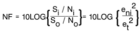
Looking at the two parts of the NF expression (inside the log function) yields:
- Si/ So→ Inverse of the power gain provided by the amplifier
- No/ Ni→ Total output noise power, including the contribution of RS, divided by the noise power at the input due to RS
To simplify this, consider Na as the noise power added by the amplifier (reflected to its input port):
- Si/ So→ 1/ G
- No/ Ni→ G * (Ni+Na) / Ni (where G*(Ni +Na ) = No)
Substituting these two expressions into the NF expression:
The noise figure expression has simplified to depend only on the ratio of the noise power added by the amplifier at its input (considering the source resistor to be in place but noiseless in getting Na) to the noise power delivered by the source resistor (considering all amplifier elements to be in place but noiseless in getting Ni).
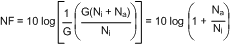
For a given amplifier with a desired closed loop gain, to minimize noise figure:
- Minimize Rf || Rg
- Choose the Optimum RS (ROPT)
ROPT is the point at which the NF curve reaches a minimum and is approximated by:
Figure 58 is a plot of NF vs RS with the circuit of Figure 52 (Rf = 240 Ω, AV = +10V/V). The NF curves for both Unterminated (RT = open) and Terminated systems (RT = RS) are shown. Table 1 indicates NF for various source resistances including RS = ROPT.
| f > 1 MHz | ||
Table 1. Noise Figure for Various Rs
| RS (Ω) | NF (TERMINATED) (dB) | NF (UNTERMINATED) (dB) |
|---|---|---|
| 50 | 8 | 3.2 |
| ROPT | 4.1 (ROPT = 750 Ω) |
1.1 (ROPT = 350 Ω) |
7.3.6 Single-Supply Operation
The LMH6629 can be operated with single power supply as shown in Figure 59. Both the input and output are capacitively coupled to set the DC operating point.
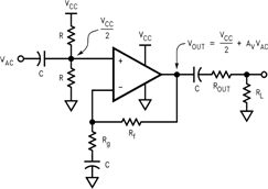 Figure 59. Single-Supply Operation
7.3.7 Low-Noise Transimpedance Amplifier
Figure 60 implements a high-speed, single-supply, low-noise Transimpedance amplifier commonly used with photo-diodes. The transimpedance gain is set by RF.
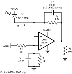 Figure 60. 200 MHz Transimpedance Amplifier Configuration
Figure 61 shows the Noise Gain (NG) and transfer function (I-V Gain). As with most Transimpedance amplifiers, it is required to compensate for the additional phase lag (Noise Gain zero at fZ) created by the total input capacitance ( CD (diode capacitance) + CCM (LMH6629 CM input capacitance) + CDIFF (LMH6629 DIFF input capacitance) ) looking into RF. This is accomplished by placing CF across RF to create enough phase lead (Noise Gain pole at fP) to stabilize the loop.
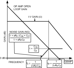 Figure 61. Transimpedance Amplifier Noise Gain and Transfer Function
The optimum value of CF is given by Equation 8 resulting in the I-V -3dB bandwidth shown in Equation 9, or around 200 MHz in this case (assuming GBWP= 4GHz with COMP pin = HI for WSON-8 package). This CF value is a “starting point” and CF needs to be tuned for the particular application as it is often less than 1 pF and thus is easily affected by board parasitics. For maximum speed, the LMH6629 COMP pin should be HI (or use the SOT-23 package).
Optimum CF Value:

Resulting -3dB Bandwidth

Equation 10 provides the total input current noise density (ini) equation for the basic Transimpedance configuration and is plotted against feedback resistance (RF) showing all contributing noise sources in Figure 62. The plot indicates the expected total equivalent input current noise density (ini) for a given feedback resistance (RF). This is depicted in the schematic of Figure 63 where total equivalent current noise density (ini) is shown at the input of a noiseless amplifier and noiseless feedback resistor (RF). The total equivalent output voltage noise density (eno) is ini*RF.
Noise Equation for Transimpedance Amplifier:
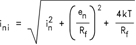
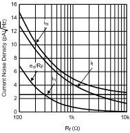 Figure 62. Current Noise Density vs. Feedback Resistance
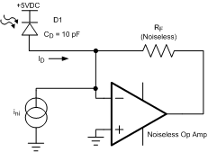 Figure 63. Transimpedance Amplifier Equivalent Input Source Model
From Figure 62, it is clear that with LMH6629’s extremely low-noise characteristics, for RF < 2.5 kΩ, the noise performance is entirely dominated by RF thermal noise. Only above this RF threshold, LMH6629’s input noise current (in) starts being a factor and at no RF setting does the LMH6629 input noise voltage play a significant role. This noise analysis has ignored the possible noise gain increase, due to photo-diode capacitance, at higher frequencies.
7.3.8 Low-Noise Integrator
Figure 64 shows a deBoo integrator implemented with the LMH6629. Positive feedback maintains integration linearity. The LMH6629’s low input offset voltage and matched inputs allow bias current cancellation and provide for very precise integration. Keeping RG and RS low helps maintain dynamic stability.
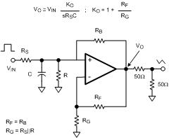 Figure 64. Low-Noise Integrator
7.3.9 High-Gain Sallen-Key Active Filters
The LMH6629 is well suited for high-gain Sallen-Key type of active filters. Figure 65 shows the 2nd order Sallen-Key low-pass filter topology. Using component predistortion methods discussed in OA-21, Component Pre-Distortion for Sallen Key Filters (SNOA369), enables the proper selection of components for these high-frequency filters.
 Figure 65. Low Pass Sallen-Key Active Filter Topology
7.4 Device Functional Modes
With an industry-leading low noise voltage operating off a supply voltage as low as 2.7-V and a common mode input voltage range that extends 0.3 V below V−, the LMH6629 finds applications in single supply, high bandwidth, ultra-low noise applications. With a GBWP of 4GHz, the LMH6629 can operate at large gains and deliver exceptional speed and low noise. Choose the WSON(8) package for the ultimate flexibility (including Power Down and COMP pin which allows tailoring internal compensation to the operating gain conditions), or the SOT23-5 package if Power Down is not needed and closed loop gain is ≥ 20dB.