SNOSA83I August 2003 – August 2014 LMH6723 , LMH6724
PRODUCTION DATA.
- 1 Features
- 2 Applications
- 3 Description
- 4 Revision History
- 5 Pin Configuration and Functions
- 6 Specifications
- 7 Application and Implementation
- 8 Power Supply Recommendations
- 9 Device and Documentation Support
- 10Mechanical, Packaging, and Orderable Information
Package Options
Mechanical Data (Package|Pins)
Thermal pad, mechanical data (Package|Pins)
Orderable Information
7 Application and Implementation
7.1 Application Information
The LMH6723/LMH6724 is a high speed current feedback amplifier manufactured on Texas Instruments' VIP10 (Vertically Integrated PNP) complimentary bipolar process. LMH6723/LMH6724 offers a unique combination of high speed and low quiescent supply current making it suitable for a wide range of battery powered and portable applications that require high performance. This amplifier can operate from 4.5V to 12V nominal supply voltages and draws only 1 mA of quiescent supply current at 10V supplies (±5V typically). The LMH6723/LMH6724 has no internal ground reference so single or split supply configurations are both equally useful.
7.2 Typical Application
7.3 Evaluation Boards
Texas Instruments provides the following evaluation boards as a guide for high frequency layout and as an aid in device testing and characterization. Many of the datasheet plots were measured with these boards.
| DEVICE | PACKAGE | BOARD PART NUMBER |
| LMH6723MA | SOIC-8 | LMH730227 |
| LMH6723MF | SOT-23 | LMH730216 |
| LMH6724MA | SOIC-8 | LMH730036 |
7.4 Feedback Resistor Selection
One of the key benefits of a current feedback operational amplifier is the ability to maintain optimum frequency response independent of gain by using appropriate values for the feedback resistor (RF). The Electrical Characteristics and Typical Performance plots were generated with an RF of 1200Ω, a gain of +2V/V and ±5V or ±2.5V power supplies (unless otherwise specified). Generally, lowering RF from its recommended value will peak the frequency response and extend the bandwidth; however, increasing the value of RF will cause the frequency response to roll off faster. Reducing the value of RF too far below it's recommended value will cause overshoot, ringing, and eventually, oscillation.
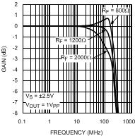 Figure 31. Frequency Response vs. RF
Figure 31 shows the LMH6723/LMH6724's frequency response as RF is varied (RL = 100Ω, AV = +2). This plot shows that an RF of 800Ω results in peaking. An RF of 1200Ω gives near maximal bandwidth and gain flatness with good stability. Since each application is slightly different, it is worth experimenting to find the optimal RF for a given circuit. In general, a value of RF that produces ~0.1 dB of peaking is the best compromise between stability and maximal bandwidth. Note that it is not possible to use a current feedback amplifier with the output shorted directly to the inverting input. The buffer configuration of the LMH6723/LMH6724 requires a 2000-Ω feedback resistor for stable operation. For other gains see the charts Figure 32 and Figure 33. These charts provide a good place to start when selecting the best feedback resistor value for a variety of gain settings.
For more information see Application Note OA-13 which describes the relationship between RF and closed-loop frequency response for current feedback operational amplifiers. The value for the inverting input impedance for the LMH6723/LMH6724 is approximately 500 Ω. The LMH6723/LMH6724 is designed for optimum performance at gains of +1 to +5V/V and −1 to −4V/V. Higher gain configurations are still useful; however, the bandwidth will fall as gain is increased, much like a typical voltage feedback amplifier.
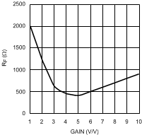 Figure 32. RF vs. Non-Inverting Gain
Figure 32 and Figure 33 show the value of RF versus gain. A higher RF is required at higher gains to keep RG from decreasing too far below the input impedance of the inverting input. This limitation applies to both inverting and non-inverting configurations. For the LMH6723/LMH6724 the input resistance of the inverting input is approximately 500Ω and 100Ω is a practical lower limit for RG. The LMH6723/LMH6724 begins to operate in a gain bandwidth limited fashion in the region where RF must be increased for higher gains. Note that the amplifier will operate with RG values well below 100 Ω; however, results will be substantially different than predicted from ideal models. In particular, the voltage potential between the Inverting and Non-Inverting inputs cannot be expected to remain small.
For inverting configurations the impedance seen by the source is RG || RT. For most sources this limits the maximum inverting gain since RF is determined by the desired gain as shown in Figure 33. The value of RG is then RF/Gain. Thus for an inverting gain of −4 V/V the input impedance is equal to 100Ω. Using a termination resistor, this can be brought down to match a 50-Ω or 75-Ω source; however, a 150Ω source cannot be matched without a severe compromise in RF.
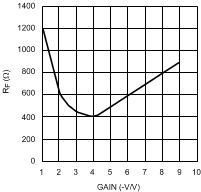 Figure 33. RF vs. Inverting Gain
7.5 Active Filters
When using any current feedback operational amplifier as an active filter it is necessary to be careful using reactive components in the feedback loop. Reducing the feedback impedance, especially at higher frequencies, will almost certainly cause stability problems. Likewise capacitance on the inverting input should be avoided. See Application Notes OA-07 and OA-26 for more information on Active Filter applications for Current Feedback Op Amps.
When using the LMH6723/LMH6724 as a low-pass filter the value of RF can be substantially reduced from the value recommended in the RF vs. Gain charts. The benefit of reducing RF is increased gain at higher frequencies, which improves attenuation in the stop band. Stability problems are avoided because in the stop band additional device bandwidth is used to cancel the input signal rather than amplify it. The benefit of this change depends on the particulars of the circuit design. With a high pass filter configuration reducing RF will likely result in device instability and is not recommended.
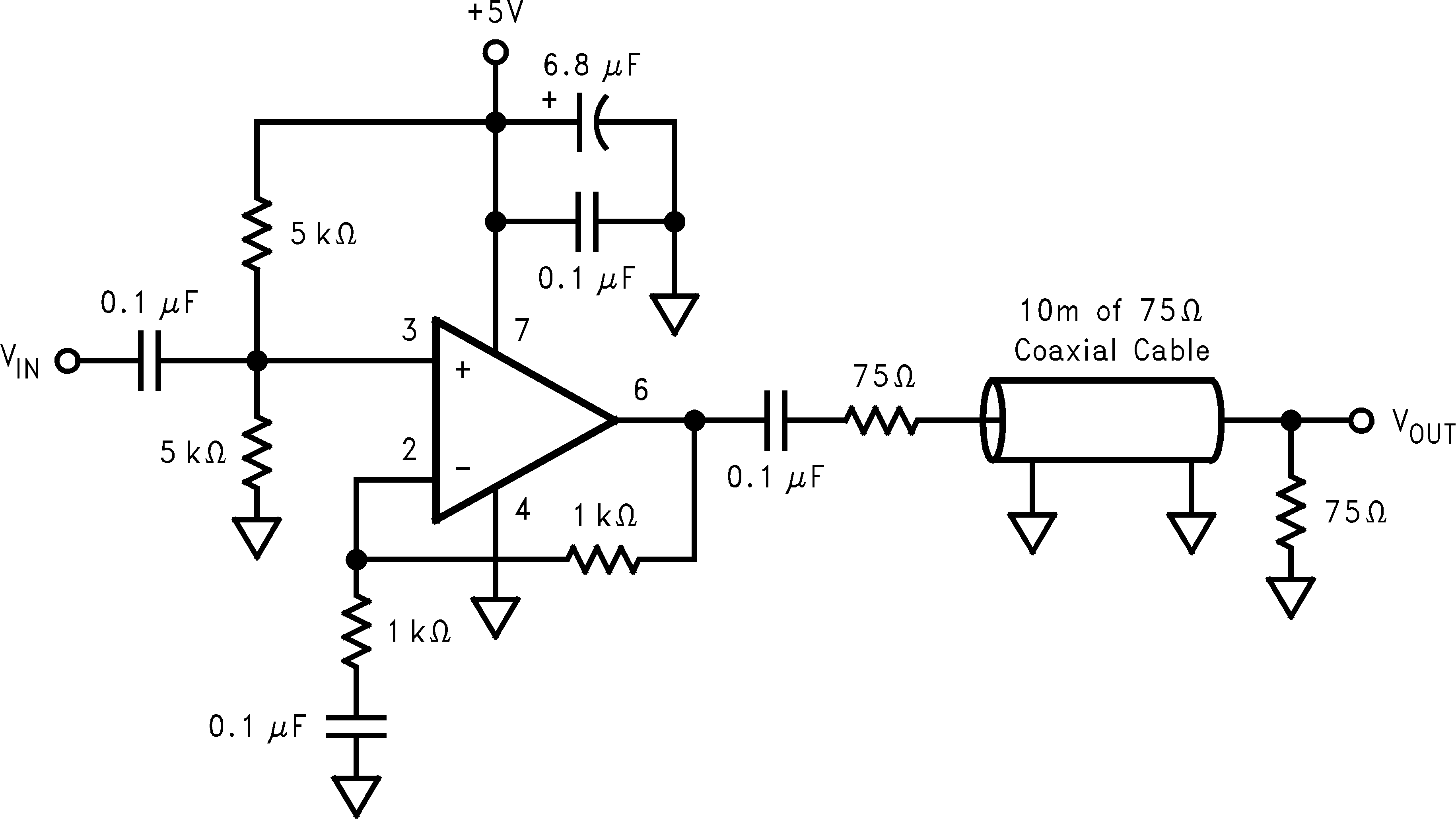
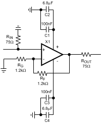 Figure 34. Typical Application with Suggested Supply Bypassing
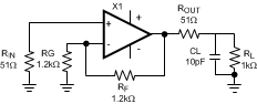 Figure 35. Decoupling Capacitive Loads
7.6 Driving Capacitive Loads
Capacitive output loading applications will benefit from the use of a series output resistor as shown in Figure 35. The charts "Suggested ROUT vs. Cap Load" give a recommended value for selecting a series output resistor for mitigating capacitive loads. The values suggested in the charts are selected for .5 dB or less of peaking in the frequency response. This gives a good compromise between settling time and bandwidth. For applications where maximum frequency response is needed and some peaking is tolerable, the value of ROUT can be reduced slightly from the recommended values.
There will be amplitude lost in the series resistor unless the gain is adjusted to compensate; this effect is most noticeable with heavy loads (RL < 150Ω).
An alternative approach is to place ROUT inside the feedback loop as shown in Figure 36. This will preserve gain accuracy, but will still limit maximum output voltage swing.
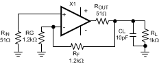 Figure 36. Series Output Resistor Inside Feedback Loop
7.7 Inverting Input Parasitic Capacitance
Parasitic capacitance is any capacitance in a circuit that was not intentionally added. It is produced through electrical interaction between conductors and can be reduced but never entirely eliminated. Most parasitic capacitances that cause problems are related to board layout or lack of termination on transmission lines. See Layout Considerations for hints on reducing problems due to parasitic capacitances on board traces. Transmission lines should be terminated in their characteristic impedance at both ends.
High speed amplifiers are sensitive to capacitance between the inverting input and ground or power supplies. This shows up as gain peaking at high frequency. The capacitor raises device gain at high frequencies by making RG appear smaller. Capacitive output loading will exaggerate this effect.
One possible remedy for this effect is to slightly increase the value of the feedback (and gain set) resistor. This will tend to offset the high frequency gain peaking while leaving other parameters relatively unchanged. If the device has a capacitive load as well as inverting input capacitance, using a series output resistor as described in Driving Capacitive Loads will help.
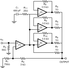 Figure 37. High Output Current Composite Amplifier
When higher currents are required than a single amplifier can provide, the circuit of Figure 37 can be used. Careful attention to a few key components will optimize performance from this circuit. The first thing to note is that the buffers need slightly higher value feedback resistors than if the amplifiers were individually configured. As well, R11 and C1 provide mid circuit frequency compensation to further improve stability. The composite amplifier has approximately twice the phase delay of a single circuit. The larger values of R8, R9 and R10, as well as the high frequency attenuation provided by C1 and R11, ensure that the circuit does not oscillate.
Resistors R4, R5, R6, and R7 are necessary to ensure even current distribution between the amplifiers. Since they are inside the feedback loop they have no effect on the gain of the circuit. The circuit shown in Figure 37 has a gain of 5. The frequency response of this circuit is shown in Figure 38.
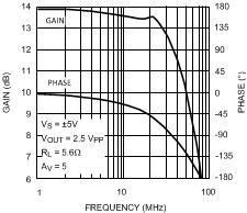 Figure 38. Composite Amplifier Frequency Response
7.8 Layout Considerations
Whenever questions about layout arise, use the evaluation board as a guide. Evaluation boards are shipped with sample requests.
To reduce parasitic capacitances ground and power planes should be removed near the input and output pins. Components in the feedback loop should be placed as close to the device as possible. For long signal paths controlled impedance lines should be used, along with impedance matching at both ends.
Bypass capacitors should be placed as close to the device as possible. Bypass capacitors from each rail to ground are applied in pairs. The larger electrolytic bypass capacitors can be located anywhere on the board; however, the smaller ceramic capacitors should be placed as close to the device as possible.
7.9 Video Performance
The LMH6723/LMH6724 has been designed to provide good performance with both PAL and NTSC composite video signals. The LMH6723/LMH6724 is specified for PAL signals. Typically, NTSC performance is marginally better due to the lower frequency content of the signal. Performance degrades as the loading is increased; therefore, best performance will be obtained with back terminated loads. The back termination reduces reflections from the transmission line and effectively masks transmission line and other parasitic capacitances from the amplifier output stage. Figure 34 shows a typical configuration for driving a 75Ω cable. The amplifier is configured for a gain of 2 to make up for the 6dB of loss in ROUT.
7.10 Single 5-V Supply Video
With a 5V supply the LMH6723/LMH6724 is able to handle a composite NTSC video signal, provided that the signal is AC coupled and level shifted so that the signal is centered around VCC/2.