SNOSA71L October 2004 – September 2015 LMP2011 , LMP2012
PRODUCTION DATA.
- 1 Features
- 2 Applications
- 3 Description
- 4 Revision History
- 5 Pin Configuration and Functions
-
6 Specifications
- 6.1 Absolute Maximum Ratings
- 6.2 ESD Ratings
- 6.3 Recommended Operating Conditions
- 6.4 Thermal Information: LMP2011
- 6.5 Thermal Information: LMP2012
- 6.6 2.7-V DC Electrical Characteristics
- 6.7 2.7-V AC Electrical Characteristics
- 6.8 5-V DC Electrical Characteristics
- 6.9 5-V AC Electrical Characteristics
- 6.10 Typical Characteristics
- 7 Detailed Description
- 8 Application and Implementation
- 9 Power Supply Recommendations
- 10Layout
- 11Device and Documentation Support
- 12Mechanical, Packaging, and Orderable Information
Package Options
Mechanical Data (Package|Pins)
Thermal pad, mechanical data (Package|Pins)
- DGK|8
Orderable Information
8 Application and Implementation
NOTE
Information in the following applications sections is not part of the TI component specification, and TI does not warrant its accuracy or completeness. TI’s customers are responsible for determining suitability of components for their purposes. Customers should validate and test their design implementation to confirm system functionality.
8.1 Application Information
The LMV201x family offers excellent dc precision and ac performance. These devices offer true rail-to-rail output, ultralow offset voltage and offset voltage drift over the entire –40 to 125°C temperature range, as well as 3-MHz bandwidth and no 1/f noise. These features make the LMV201x a robust, high performance operational amplifier ideal for industrial applications.
8.2 Typical Applications
8.2.1 Extending Supply Voltages and Output Swing with a Composite Amplifier
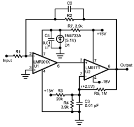
 Figure 31. Inverting Composite Amplifier
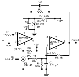
 Figure 32. Non-Inverting Composite Amplifier
8.2.1.1 Design Requirements
In cases where substantially higher output swing is required with higher supply voltages, arrangements like the ones shown in Figure 31 and Figure 32 could be used. These configurations utilize the excellent DC performance of the LMP201x while at the same time allow the superior voltage and frequency capabilities of the LM6171 to set the dynamic performance of the overall amplifier.
For example, it is possible to achieve ±12-V output swing with 300 MHz of overall GBW (AV = 100) while keeping the worst case output shift due to VOS less than 4 mV.
8.2.1.2 Detailed Design Procedure
The LMP201x output voltage is kept at about mid-point of its overall supply voltage, and its input common mode voltage range allows the V- terminal to be grounded in one case (Figure 31, inverting operation) and tied to a small non-critical negative bias in another (Figure 32, non-inverting operation). Higher closed-loop gains are also possible with a corresponding reduction in realizable bandwidth. Table 1 shows some other closed loop gain possibilities along with the measured performance in each case.
In terms of the measured output peak-to-peak noise, the following relationship holds between output noise voltage, en p-p, for different closed-loop gain, AV, settings, where −3 dB Bandwidth is BW:

It should be kept in mind that in order to minimize the output noise voltage for a given closed-loop gain setting, one could minimize the overall bandwidth. As can be seen from Equation 1 above, the output noise has a square-root relationship to the Bandwidth.
In the case of the inverting configuration, it is also possible to increase the input impedance of the overall amplifier, by raising the value of R1, without having to increase the feed-back resistor, R2, to impractical values, by utilizing a "Tee" network as feedback. See the LMC6442 data sheet (Application Notes section) for more details on this.
8.2.1.3 Application Results
Table 1 shows the results using various gains and compensation values.
Table 1. Composite Amplifier Measured Performance
| AV | R1 (Ω) |
R2 (Ω) |
C2 (pF) |
BW (MHz) |
SR (V/μs) |
en p-p (mVPP) |
|---|---|---|---|---|---|---|
| 50 | 200 | 10k | 8 | 3.3 | 178 | 37 |
| 100 | 100 | 10k | 10 | 2.5 | 174 | 70 |
| 100 | 1k | 100k | 0.67 | 3.1 | 170 | 70 |
| 500 | 200 | 100k | 1.75 | 1.4 | 96 | 250 |
| 1000 | 100 | 100k | 2.2 | 0.98 | 64 | 400 |
8.2.2 Precision Strain-gauge Amplifier
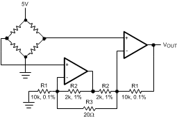
 Figure 33. Precision Strain Gauge Amplifier
This Strain-Gauge amplifier (Figure 33) provides high gain (1006 or ~60 dB) with very low offset and drift. Using the resistors' tolerances as shown, the worst case CMRR will be greater than 108 dB. The CMRR is directly related to the resistor mismatch. The rejection of common-mode error, at the output, is independent of the differential gain, which is set by R3. The CMRR is further improved, if the resistor ratio matching is improved, by specifying tighter-tolerance resistors, or by trimming.
8.2.3 ADC Input Amplifier
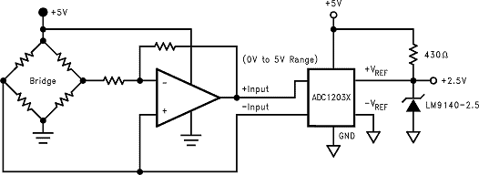
The LMP201x is a great choice for an amplifier stage immediately before the input of an ADC (Analog-to-Digital Converter). See Figure 34.
This is because of the following important characteristics:
- Very low offset voltage and offset voltage drift over time and temperature allow a high closed-loop gain setting without introducing any short-term or long-term errors. For example, when set to a closed-loop gain of 100 as the analog input amplifier for a 12-bit A/D converter, the overall conversion error over full operation temperature and 30 years life of the part (operating at 50°C) would be less than 5 LSBs.
- Fast large-signal settling time to 0.01% of final value (1.4 μs) allows 12 bit accuracy at 100 KHZ or more sampling rate
- No flicker (1/f) noise means unsurpassed data accuracy over any measurement period of time, no matter how long. Consider the following op amp performance, based on a typical low-noise, high-performance commercially-available device, for comparison:
- Op amp flatband noise = 8 nV/√Hz
- 1/f corner frequency = 100 Hz
- AV = 2000
- Measurement time = 100 sec
- Bandwidth = 2 Hz
- This example will result in about 2.2 mVPP (1.9 LSB) of output noise contribution due to the op amp alone, compared to about 594 μVPP (less than 0.5 LSB) when that op amp is replaced with the LMP201x which has no 1/f contribution. If the measurement time is increased from 100 seconds to 1 hour, the improvement realized by using the LMP201x would be a factor of about 4.8 times (2.86 mVPP compared to 596 μV when LMP201x is used) mainly because the LMP201x accuracy is not compromised by increasing the observation time.
- Copper leadframe construction minimizes any thermocouple effects which would degrade low level/high gain data conversion application accuracy (see discussion under The Benefits of the LMP201X section above).
- Rail-to-Rail output swing maximizes the ADC dynamic range in 5-Volt single-supply converter applications. Below is a typical block diagram showing the LMP201x used as an ADC amplifier (Figure 34).
