SNOSAI9I September 2005 – November 2015 LMP7701 , LMP7702 , LMP7704
PRODUCTION DATA.
- 1 Features
- 2 Applications
- 3 Description
- 4 Revision History
- 5 Description (continued)
- 6 Pin Configuration and Functions
- 7 Specifications
- 8 Detailed Description
- 9 Application and Implementation
- 10Power Supply Recommendations
- 11Layout
- 12Device and Documentation Support
- 13Mechanical, Packaging, and Orderable Information
Package Options
Mechanical Data (Package|Pins)
Thermal pad, mechanical data (Package|Pins)
Orderable Information
9 Application and Implementation
NOTE
Information in the following applications sections is not part of the TI component specification, and TI does not warrant its accuracy or completeness. TI’s customers are responsible for determining suitability of components for their purposes. Customers should validate and test their design implementation to confirm system functionality.
9.1 Application Information
9.1.1 Low Input Voltage Noise
The LMP770x have the very low input voltage noise of 9 nV/√Hz. This input voltage noise can be further reduced by placing N amplifiers in parallel as shown in Figure 46. The total voltage noise on the output of this circuit is divided by the square root of the number of amplifiers used in this parallel combination. This is because each individual amplifier acts as an independent noise source, and the average noise of independent sources is the quadrature sum of the independent sources divided by the number of sources. For N identical amplifiers, this means:

Figure 46 shows a schematic of this input voltage noise reduction circuit. Typical resistor values are:
RG = 10Ω, RF = 1 kΩ, and RO = 1 kΩ.
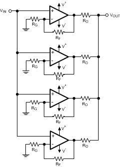 Figure 46. Noise Reduction Circuit
9.1.2 Total Noise Contribution
The LMP770x have very low input bias current, very low input current noise, and very low input voltage noise. As a result, these amplifiers are ideal choices for circuits with high impedance sensor applications.
Figure 47 shows the typical input noise of the LMP770x as a function of source resistance where:
en denotes the input referred voltage noise
ei is the voltage drop across source resistance due to input referred current noise or ei = RS * in
et shows the thermal noise of the source resistance
eni shows the total noise on the input.
Where:
The input current noise of the LMP770x is so low that it will not become the dominant factor in the total noise unless source resistance exceeds 300 MΩ, which is an unrealistically high value.
As is evident in Figure 47, at lower RS values, total noise is dominated by the amplifier's input voltage noise. Once RS is larger than a few kilo-Ohms, then the dominant noise factor becomes the thermal noise of RS. As mentioned before, the current noise will not be the dominant noise factor for any practical application.
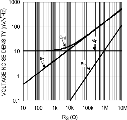 Figure 47. Total Input Noise
9.2 Typical Application
9.2.1 Design Requirements
pH electrodes are very high impedance sensors. As their name indicates, they are used to measure the pH of a solution. They usually do this by generating an output voltage which is proportional to the pH of the solution. pH electrodes are calibrated so that they have zero output for a neutral solution, pH = 7, and positive and negative voltages for acidic or alkaline solutions. This means that the output of a pH electrode is bipolar and must be level shifted to be used in a single supply system. The rate of change of this voltage is usually shown in mV/pH and is different for different pH sensors. Temperature is also an important factor in a pH electrode reading. The output voltage of the senor will change with temperature.
9.2.2 Detailed Design Procedure
Many sensors have high source impedances that may range up to 10 MΩ. The output signal of sensors often needs to be amplified or otherwise conditioned by means of an amplifier. The input bias current of this amplifier can load the sensor's output and cause a voltage drop across the source resistance as shown in Figure 49, where VIN+ = VS – IBIAS*RS
The last term, IBIAS*RS, shows the voltage drop across RS. To prevent errors introduced to the system due to this voltage, an op amp with very low input bias current must be used with high impedance sensors. This is to keep the error contribution by IBIAS*RS less than the input voltage noise of the amplifier, so that it will not become the dominant noise factor.
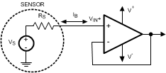 Figure 49. Noise Due to IBIAS
Figure 50 shows a typical output voltage spectrum of a pH electrode. The exact values of output voltage will be different for different sensors. In this example, the pH electrode has an output voltage of 59.15 mV/pH at 25°C.
 Figure 50. Output Voltage of a pH Electrode
The temperature dependence of a typical pH electrode is shown in Figure 51. As is evident, the output voltage changes with changes in temperature.
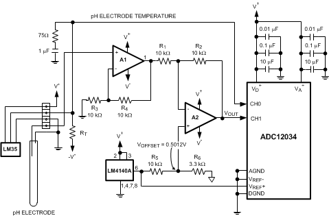
The schematic shown in Figure 48 is a typical circuit which can be used for pH measurement. The LM35 is a precision integrated circuit temperature sensor. This sensor is differentiated from similar products because it has an output voltage linearly proportional to Celcius measurement, without converting the temperature to Kelvin. The LM35 is used to measure the temperature of the solution and feeds this reading to the Analog to Digital Converter, ADC. This information is used by the ADC to calculate the temperature effects on the pH readings. The LM35 needs to have a resistor, RT in Figure 48, to –V+ to be able to read temperatures less than 0°C. RT is not needed if temperatures are not expected to be less than zero.
The output of pH electrodes is usually large enough that it does not require much amplification; however, due to the very high impedance, the output of a pH electrode needs to be buffered before it can go to an ADC. Because most ADCs are operated on single supply, the output of the pH electrode also needs to be level shifted. Amplifier A1 buffers the output of the pH electrode with a moderate gain of +2, while A2 provides the level shifting. VOUT at the output of A2 is given by: VOUT = −2VpH + 1.024V.
The LM4140A is a precision, low noise, voltage reference used to provide the level shift needed. The ADC used in this application is the ADC12032 which is a 12-bit, 2 channel converter with multiplexers on the inputs and a serial output. The 12-bit ADC enables users to measure pH with an accuracy of 0.003 of a pH unit. Adequate power supply bypassing and grounding is extremely important for ADCs. Recommended bypass capacitors are shown in Figure 48. It is common to share power supplies between different components in a circuit. To minimize the effects of power supply ripples caused by other components, the op amps must have bypass capacitors on the supply pins. Using the same value capacitors as those used with the ADC are ideal. The combination of these three values of capacitors ensures that AC noise present on the power supply line is grounded and does not interfere with the amplifiers' signal.
9.2.3 Application Curves
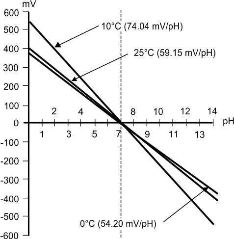 Figure 51. Temperature Dependence of a pH Electrode
