SNOSAW6E January 2008 – December 2014 LMP7721
PRODUCTION DATA.
- 1 Features
- 2 Applications
- 3 Description
- 4 Revision History
- 5 Pin Configuration and Functions
- 6 Specifications
- 7 Detailed Description
- 8 Application and Implementation
- 9 Power Supply Recommendations
- 10Layout
- 11Device and Documentation Support
- 12Mechanical, Packaging, and Orderable Information
Package Options
Mechanical Data (Package|Pins)
- D|8
Thermal pad, mechanical data (Package|Pins)
Orderable Information
6 Specifications
6.1 Absolute Maximum Ratings(1)(4)
| MIN | MAX | UNIT | |
|---|---|---|---|
| VIN Differential | –0.3 | 0.3 | V |
| Supply Voltage (VS = V+ – V−) (3) | –0.3 | 6.0 | V |
| Voltage on Input/Output Pins | V+ + 0.3 | V− − 0.3 | V |
| Junction Temperature (2) | 150 | °C | |
| Soldering Information | |||
| Infrared or Convection (20 sec) | 235 | °C | |
| Wave Soldering Lead Temp. (10 sec) | 260 | °C | |
| Storage temperature, Tstg | −65 | 150 | °C |
(1) Absolute Maximum Ratings indicate limits beyond which damage to the device may occur. Recommended Operating Conditions indicate conditions for which the device is intended to be functional, but specific performance is not ensured. For ensured specifications and the test conditions, see the Electrical Characteristics Tables.
(2) The maximum power dissipation is a function of TJ(MAX), θJA. The maximum allowable power dissipation at any ambient temperature is PD = (TJ(MAX) - TA)/θJA. All numbers apply for packages soldered directly onto a PC Board.
(3) The voltage on any pin should not exceed 6V relative to any other pins.
(4) If Military/Aerospace specified devices are required, please contact the Texas Instruments Sales Office/Distributors for availability and specifications.
6.2 ESD Ratings
| VALUE | UNIT | |||
|---|---|---|---|---|
| V(ESD) | Electrostatic discharge | Human-body model (HBM), per ANSI/ESDA/JEDEC JS-001(1) | ±2000 | V |
| Charged-device model (CDM), per JEDEC specification JESD22-C101(2) | ±200 | |||
(1) JEDEC document JEP155 states that 500-V HBM allows safe manufacturing with a standard ESD control process.
(2) JEDEC document JEP157 states that 250-V CDM allows safe manufacturing with a standard ESD control process.
6.3 Recommended Operating Conditions
| MIN | MAX | UNIT | |
|---|---|---|---|
| Temperature Range(2) | –40 | 125 | °C |
| Supply Voltage (VS = V+ – V−): | |||
| 0°C ≤ TA ≤ 125°C | 1.8 | 5.5 | V |
| −40°C ≤ TA ≤ 125°C | 2.0 | 5.5 | V |
6.4 Thermal Information
| THERMAL METRIC(1) | LMP7721 | UNIT | |
|---|---|---|---|
| D | |||
| 8 PINS | |||
| RθJA | Junction-to-ambient thermal resistance | 190 | °C/W |
(1) For more information about traditional and new thermal metrics, see the IC Package Thermal Metrics application report, SPRA953.
6.5 Electrical Characteristics: 2.5 V
Unless otherwise specified, all limits are specified for TA = 25°C, V+ = 2.5 V, V− = 0 V, VCM = (V+ + V−)/2.| PARAMETER | TEST CONDITIONS | MIN(2) | TYP(1) | MAX(2) | UNIT | ||
|---|---|---|---|---|---|---|---|
| VOS | Input Offset Voltage | –180 | ±50 | 180 | μV | ||
| –40°C ≤ TJ ≤ 125°C | –480 | 480 | |||||
| TC VOS | Input Offset Voltage Drift (3) |
–1.5 | –4 | μV/°C | |||
| IBIAS | Input Bias Current | VCM = 1 V(4)(5) | 25°C | –20 | ±3 | 20 | fA |
| −40°C to 85°C | –900 | 900 | |||||
| −40°C to 125°C | –5 | 5 | pA | ||||
| IOS | Input Offset Current | VCM = 1 V(5) | ±6 | ±40 | fA | ||
| CMRR | Common-Mode Rejection Ratio | 0 V ≤ VCM ≤ 1.4 V | 83 | 100 | dB | ||
| 0 V ≤ VCM ≤ 1.4 V, –40°C ≤ TJ ≤ 125°C | 80 | ||||||
| PSRR | Power Supply Rejection Ratio | 1.8 V ≤ V+ ≤ 5.5 V, V− = 0 V, VCM = 0 | 84 | 92 | dB | ||
| 1.8 V ≤ V+ ≤ 5.5 V, V− = 0 V, VCM = 0, –40°C ≤ TJ ≤ 125°C | 80 | ||||||
| CMVR | Input Common-Mode Voltage Range | CMRR ≥ 80 dB | −0.3 | 1.5 | V | ||
| CMRR ≥ 78 dB, –40°C ≤ TJ ≤ 125°C | –0.3 | 1.5 | |||||
| AVOL | Large Signal Voltage Gain | VO = 0.15 V to 2.2 V, RL = 2 kΩ to V+/2 | 88 | 107 | dB | ||
| VO = 0.15 V to 2.2 V, RL = 2 kΩ to V+/2, –40°C ≤ TJ ≤ 125°C | 82 | ||||||
| VO = 0.15 V to 2.2 V, RL = 10 kΩ to V+/2 | 92 | 120 | |||||
| VO = 0.15 V to 2.2 V, RL = 10 kΩ to V+/2, –40°C ≤ TJ ≤ 125°C | 88 | ||||||
| VO | Output Swing High | RL = 2 kΩ to V+/2 | 70 | 25 | mV from V+ |
||
| RL = 2 kΩ to V+/2, –40°C ≤ TJ ≤ 125°C | 77 | ||||||
| RL = 10 kΩ to V+/2 | 60 | 20 | |||||
| RL = 10 kΩ to V+/2, –40°C ≤ TJ ≤ 125°C | 66 | ||||||
| Output Swing Low | RL = 2 kΩ to V+/2 | 30 | 70 | mV | |||
| RL = 2 kΩ to V+/2, –40°C ≤ TJ ≤ 125°C | 73 | ||||||
| RL = 10 kΩ to V+/2 | 15 | 60 | |||||
| RL = 10 kΩ to V+/2, –40°C ≤ TJ ≤ 125°C | 62 | ||||||
| IO | Output Short Circuit Current | Sourcing to V−, VIN = 200 mV (6) | 36 | 46 | mA | ||
| Sourcing to V−, VIN = 200 mV (6), –40°C ≤ TJ ≤ 125°C | 30 | ||||||
| Sinking to V+, VIN = −200 mV (6) | 7.5 | 15 | |||||
| Sinking to V+, VIN = −200 mV (6), –40°C ≤ TJ ≤ 125°C | 5.0 | ||||||
| IS | Supply Current | 1.1 | 1.5 | mA | |||
| –40°C ≤ TJ ≤ 125°C | 1.75 | ||||||
| SR | Slew Rate | AV = +1, Rising (10% to 90%) | 9.3 | V/μs | |||
| AV = +1, Falling (90% to 10%) | 10.8 | ||||||
| GBW | Gain Bandwidth Product | 15 | MHz | ||||
| en | Input-Referred Voltage Noise | f = 400 Hz | 8 | nV/ |
|||
| f = 1 kHz | 7 | ||||||
| In | Input-Referred Current Noise | f = 1 kHz | 0.01 | pA/ |
|||
| THD+N | Total Harmonic Distortion + Noise | f = 1 kHz, AV = 2, RL = 100 kΩ VO = 0.9 VPP |
0.003% | ||||
| f = 1 kHz, AV = 2, RL = 600 Ω VO = 0.9 VPP |
0.003% | ||||||
6.6 Electrical Characteristics: 5 V
Unless otherwise specified, all limits are specified for TA = 25°C, V+ = 5 V, V− = 0 V, VCM = (V+ + V−)/2.| PARAMETER | TEST CONDITIONS | MIN(2) | TYP(1) | MAX(2) | UNIT | ||
|---|---|---|---|---|---|---|---|
| VOS | Input Offset Voltage | –150 | ±26 | 150 | μV | ||
| –40°C ≤ TJ ≤ 125°C | 450 | 450 | |||||
| TC VOS | Input Offset Average Drift (3) |
–1.5 | –4 | μV/°C | |||
| IBIAS | Input Bias Current | VCM = 1 V(4)(5) | 25°C | –20 | ±3 | 20 | fA |
| −40°C to 85°C | –900 | 900 | |||||
| −40°C to 125°C | –5 | 5 | pA | ||||
| IOS | Input Offset Current | (5) | ±6 | ±40 | fA | ||
| CMRR | Common-Mode Rejection Ratio | 0 V ≤ VCM ≤ 3.7 V | 84 | 100 | dB | ||
| 0 V ≤ VCM ≤ 3.7 V, –40°C ≤ TJ ≤ 125°C | 82 | ||||||
| PSRR | Power Supply Rejection Ratio | 1.8 V ≤ V+ ≤ 5.5 V, V− = 0 V, VCM = 0 | 84 | 96 | dB | ||
| 1.8 V ≤ V+ ≤ 5.5 V, V− = 0 V, VCM = 0, –40°C ≤ TJ ≤ 125°C | 80 | ||||||
| CMVR | Input Common-Mode Voltage Range | CMRR ≥ 80 dB | −0.3 | 4 | V | ||
| CMRR ≥ 78 dB, –40°C ≤ TJ ≤ 125°C | –0.3 | 4 | |||||
| AVOL | Large Signal Voltage Gain | VO = 0.3 V to 4.7 V, RL = 2 kΩ to V+/2 | 88 | 111 | dB | ||
| VO = 0.3 V to 4.7 V, RL = 2 kΩ to V+/2, –40°C ≤ TJ ≤ 125°C | 82 | ||||||
| VO = 0.3 V to 4.7 V, RL = 10 kΩ to V+/2 | 92 | 120 | |||||
| VO = 0.3 V to 4.7 V, RL = 10 kΩ to V+/2, –40°C ≤ TJ ≤ 125°C | 88 | ||||||
| VO | Output Swing High | RL = 2 kΩ to V+/2 | 70 | 30 | mV from V+ |
||
| RL = 2 kΩ to V+/2, –40°C ≤ TJ ≤ 125°C | 77 | ||||||
| RL = 10 kΩ to V+/2 | 60 | 20 | |||||
| RL = 10 kΩ to V+/2, –40°C ≤ TJ ≤ 125°C | 66 | ||||||
| Output Swing Low | RL = 2 kΩ to V+/2 | 31 | 70 | mV | |||
| RL = 2 kΩ to V+/2, –40°C ≤ TJ ≤ 125°C | 73 | ||||||
| RL = 10 kΩ to V+/2 | 20 | 60 | |||||
| RL = 10 kΩ to V+/2, –40°C ≤ TJ ≤ 125°C | 62 | ||||||
| IO | Output Short Circuit Current | Sourcing to V−, VIN = 200 mV (6) | 46 | 60 | mA | ||
| Sourcing to V−, VIN = 200 mV (6), –40°C ≤ TJ ≤ 125°C | 38 | ||||||
| Sinking to V+, VIN = −200 mV (6) | 10.5 | 22 | |||||
| Sinking to V+, VIN = −200 mV (6), –40°C ≤ TJ ≤ 125°C | 6.5 | ||||||
| IS | Supply Current | 1.3 | 1.7 | mA | |||
| –40°C ≤ TJ ≤ 125°C | 1.95 | ||||||
| SR | Slew Rate | AV = +1, Rising (10% to 90%) | 10.43 | V/μs | |||
| AV = +1, Falling (90% to 10%) | 12.76 | ||||||
| GBW | Gain Bandwidth Product | 17 | MHz | ||||
| en | Input-Referred Voltage Noise | f = 400 Hz | 7.5 | nV/ |
|||
| f = 1 kHz | 6.5 | ||||||
| In | Input-Referred Current Noise | f = 1 kHz | 0.01 | pA/ |
|||
| THD+N | Total Harmonic Distortion + Noise | f = 1 kHz, AV = 2, RL = 100 kΩ VO = 4 VPP |
0.0007% | ||||
| f = 1 kHz, AV = 2, RL = 600Ω VO = 4 VPP |
0.0007% | ||||||
(1) Typical values represent the most likely parametric norm as determined at the time of characterization. Actual typical values may vary over time and will also depend on the application and configuration. The typical values are not tested and are not specified on shipped production material.
(2) Limits are 100% production tested at 25°C. Limits over the operating temperature range are specified through correlations using the Statistical Quality Control (SQC) method.
(3) Offset voltage average drift is determined by dividing the change in VOS at the temperature extremes by the total temperature change.
(4) Positive current corresponds to current flowing into the device.
(5) This parameter is specified by design and/or characterization and is not tested in production.
(6) The short circuit test is a momentary open loop test.
6.7 Typical Characteristics
Unless otherwise specified: TA = 25°C, VCM = (V+ + V−)/2.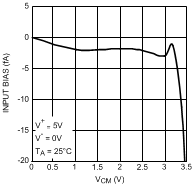 Figure 1. Input Bias Current vs. VCM
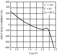 Figure 3. Input Bias Current vs. VCM
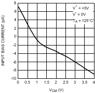 Figure 5. Input Bias Current vs. VCM
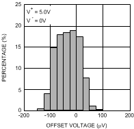 Figure 7. Offset Voltage Distribution
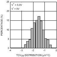 Figure 9. TCVOS Distribution
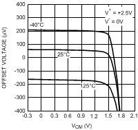 Figure 11. Offset Voltage vs. VCM
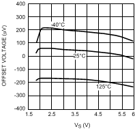 Figure 13. Offset Voltage vs. Supply Voltage
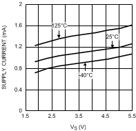 Figure 15. Supply Current vs. Supply Voltage
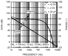 Figure 17. Open-Loop Frequency Response Gain and Phase
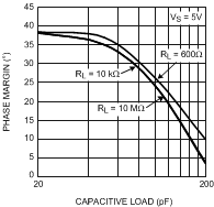 Figure 19. Phase Margin vs. Capacitive Load
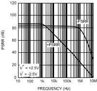 Figure 21. PSRR vs. Frequency
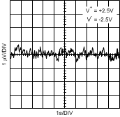 Figure 23. Time Domain Voltage Noise
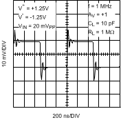 Figure 25. Small Signal Step Response
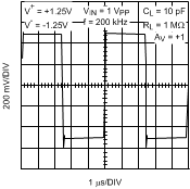 Figure 27. Large Signal Step Response
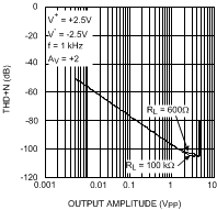 Figure 29. THD+N vs. Output Voltage
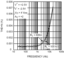 Figure 31. THD+N vs. Frequency
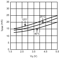 Figure 33. Sinking Current vs. Supply Voltage
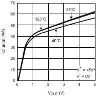 Figure 35. Sourcing Current vs. Output Voltage
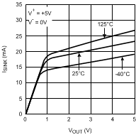 Figure 37. Sinking Current vs. Output Voltage
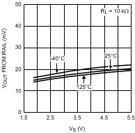 Figure 39. Output Swing Low vs. Supply Voltage
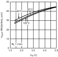 Figure 41. Output Swing Low vs. Supply Voltage
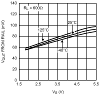 Figure 43. Output Swing Low vs. Supply Voltage
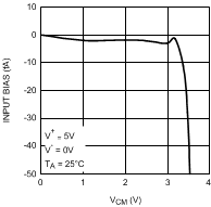 Figure 2. Input Bias Current vs. VCM
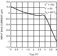 Figure 4. Input Bias Current vs. VCM
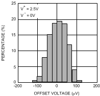 Figure 6. Offset Voltage Distribution
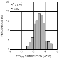 Figure 8. TCVOS Distribution
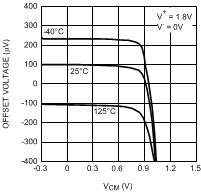 Figure 10. Offset Voltage vs. VCM
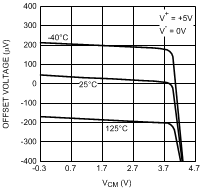 Figure 12. Offset Voltage vs. VCM
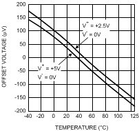 Figure 14. Offset Voltage vs. Temperature
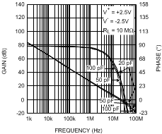 Figure 16. Open-Loop Frequency Response Gain and Phase
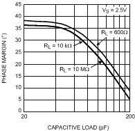 Figure 18. Phase Margin vs. Capacitive Load
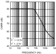 Figure 20. CMRR vs. Frequency
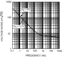 Figure 22. Input-Referred Voltage Noise vs. Frequency
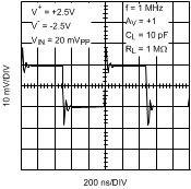 Figure 24. Small Signal Step Response
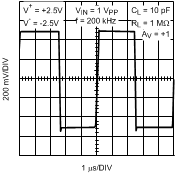 Figure 26. Large Signal Step Response
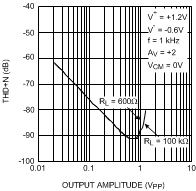 Figure 28. THD+N vs. Output Voltage
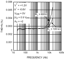 Figure 30. THD+N vs. Frequency
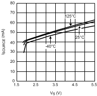 Figure 32. Sourcing Current vs. Supply Voltage
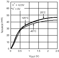 Figure 34. Sourcing Current vs. Output Voltage
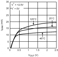 Figure 36. Sinking Current vs. Output Voltage
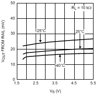 Figure 38. Output Swing High vs. Supply Voltage
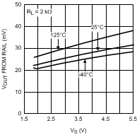 Figure 40. Output Swing High vs. Supply Voltage
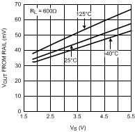 Figure 42. Output Swing High vs. Supply Voltage