SNAS634B March 2014 – January 2016 LMP92066
PRODUCTION DATA.
- 1 Features
- 2 Applications
- 3 Description
- 4 Simplified Schematic
- 5 Revision History
- 6 Pin Configuration and Functions
- 7 Specifications
-
8 Detailed Description
- 8.1 Overview
- 8.2 Functional Block Diagram
- 8.3 Features Description
- 8.4 Device Functional Modes
- 8.5
Programming
- 8.5.1 Temperature Sensor Output Data Access Registers
- 8.5.2 DAC Input Data Registers
- 8.5.3 Temperature Sensor Status Register
- 8.5.4 Override Control Register
- 8.5.5 Override Data Registers
- 8.5.6 EEPROM Control Register
- 8.5.7 Software RESET Register
- 8.5.8 Access Control Register
- 8.5.9 Block I2C Access Control Register
- 8.5.10 I2C Address LOCK Register
- 8.5.11 Output Drive Supply Status Register
- 8.5.12 Device Version Register
- 8.5.13 EEPROM Burn Counter
- 8.5.14 LUT Coefficient Registers
- 8.5.15 LUT Control Registers
- 8.5.16 Notepad Registers
- 8.6 Register Map
- 9 Application and Implementation
- 10Power Supply Recommendations
- 11Layout
- 12Device and Documentation Support
- 13Mechanical, Packaging, and Orderable Information
Package Options
Mechanical Data (Package|Pins)
- PWP|16
Thermal pad, mechanical data (Package|Pins)
- PWP|16
Orderable Information
8 Detailed Description
8.1 Overview
The LMP92066 is a dual temperature-dependent bias generator whose temperature-to-voltage transfer functions are user defined. The device contains a digital temperature sensor that addresses two independently programmable Look-Up-Tables (LUTs). The outputs of LUTs are sent on to their respective 12-bit DACs to produce two independent output voltages. For added flexibility the device can be configured to provide bias potential above or below GNDA.
In applications requiring rapid ON/OFF switching of the bias voltage, the LMP92066 provides asynchronous control over its outputs. Dedicated digital input pins control analog output switching.
All aspects of the device functionality are controlled through internal registers. These registers, and the LUTs, are accessible through the I2C-compatible interface.
The LMP92066 can operate autonomously of the system controller, once LUT coefficients have been committed to its non-volatile memory, EEPROM. Upon power up the EEPROM content is automatically transferred to the operating memory, and the device begins to produce required bias voltage.
8.2 Functional Block Diagram
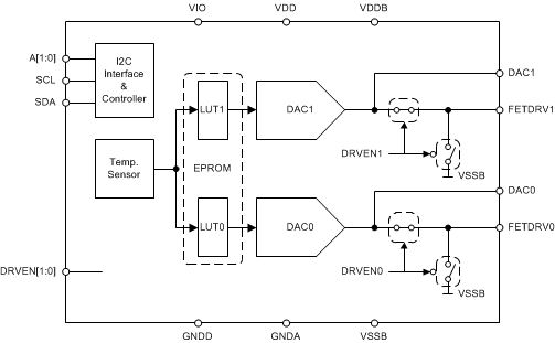
8.3 Features Description
8.3.1 Temperature Sensor
The onboard digital temperature sensor produces 12-bit, twos complement output, where the LSB represents +0.0625°C, and MSB represents –128°C. The output of the temperature sensor is stored in the TEMPM and TEMPL registers. These registers are updated automatically once the temperature sensor completes a new conversion, approximately every 25 ms. The temperature sensor begins operation immediately after the supply voltage at VDD has reached its minimum operating level. Initially, right after power up, TEMPM and TEMPL registers contain 0s. The first measurement result is loaded into TEMPM and TEMPL registers 25 ms after power up.
Table 1. Temperature Sensor Output
| TEMPERATURE SENSOR OUTPUT {TEMPM[3:0], TEMPL[7:0]} |
TEMPERATURE (°C) |
|---|---|
| 100000000000 | –128.0000 |
| 111001000000 | –28.0000 |
| 111111111111 | –0.0625 |
| 000000000001 | 0.0625 |
| 000110000000 | 24.0000 |
| 011111111111 | 127.9375 |
NOTE
The maximum output of the temperature sensor stored in the TEMPM and TEMPL registers is 127.9375°C.
8.3.2 Look-Up-Table (LUT) and Arithmetic-Logic Unit (ALU)
The LUT is used to create an arbitrary transfer function which maps the temperature to the analog output of the device. In concept, the temperature readout is used as a pointer to a table of discrete values that are representative of the samples of the desired temperature-dependent function.
In order to minimize the storage requirements, the LMP92066 LUTs are indexed in 4°C increments. Also, the stored values are only the increments, or first derivatives (Δs) of the modeled transfer function. The internal ALU reconstructs the original transfer function by integrating the coefficients stored in the LUTs. The errors due to the coarseness of the temperature quantization are significantly reduced through the use of linear interpolation, which is also implemented in the ALU.
Consider the example shown in Figure 22. The target output vs temperature is shown in the top graph. VDACx is a smooth, monotonic function with, ideally, infinite precision. The LUT stores only the increments, or the rise, within each 4°C interval.
In order to recreate the original transfer function, the series of increments must be summed together and added to the constant BASE value. BASE represents the constant offset which is lost due to the differentiation - storage of the increments only. This process must also be referenced to the common temperature point. This reference temperature is called BASELINE in this document, and is fixed at 24°C.
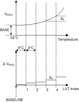 Figure 22. Original Transfer Function
The LUT and ALU Organization, LUT Coefficient to Register Mapping, and The LUT Input and Output Ranges sections below detail the operation of the LUTs and the ALUs.
8.3.2.1 LUT and ALU Organization
In Figure 23 TEMP represents the 12-bit input value to the LUT. This value is produced by the local temperature sensor, or it can be provided by the user through the use of the OVERRIDE registers. The OVERRIDE modes are described in the later sections.
TEMP is truncated, and TEMP[11:6] is used to index the LUT. The truncation is equivalent to reducing the TEMP resolution from 0.0625°C/LSB to 4°C/LSB.
The overall transfer function is stored in the LUT as a set of unsigned 4-bit increments from the BASE value, that is, LUT location (+1) stores the value of the increment Δ1. This is shown in Figure 23. The BASELINE is 24°C temperature reference point, and BASE is the numeric representation of the required output at 24°C
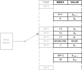 Figure 23. LUT Organization
When TEMP is above 24°C, the LUT is addressed above the BASELINE address, all increments are added to the BASE value to produce numeric equivalent of the analog output. When TEMP is below 24°C, LUT is addressed below the BASELINE, all increments are subtracted from the BASE value to produce DACIN.
Interpolation function is implemented in the ALU that follows the LUT. The truncated lower bits of the TEMP value, REM = TEMP[5:0], are used to interpolate between data points stored in the LUT. A portion of increment, αΔi, is added to form the final numeric output - the input data to the DAC. The factor α is a fraction of 4°C temperature span, or equivalently it is a fraction of the 64-code temperature span.

The process of calculating the DACIN, including the interpolation, is depicted in Figure 24. The DACIN is the final 12-bit value produced by the ALU and the LUT, and forwarded to the DAC for conversion to analog domain.
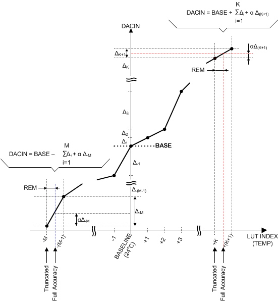 Figure 24. DACIN Calculation
Up to this point the algorithm description concerned only the generation of the monotonically increasing transfer function. The device can also produce monotonically decreasing transfer function by setting the DACx_BASEM.POL bit.
The effect of polarity reversal (POL = 1) on the overall transfer function is shown in Figure 25. The LUT content is unchanged from the original example above. Note that now the LUT values stored at locations above BASELINE address are subtracted from BASE value, and the LUT values stored at locations below BASELINE address are added to the BASE value.
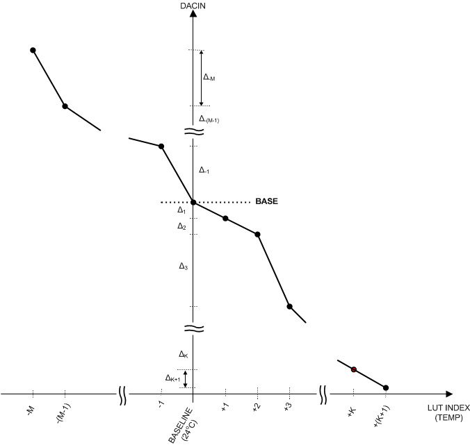 Figure 25. Monotonically Decreasing Transfer Function
The expressions used in the calculation of the transfer function are summarized below:
LUT index > BASELINE:

LUT index < BASELINE:

8.3.2.2 LUT Coefficient to Register Mapping
For the sake of convenience the preceding sections referred to LUT coefficients as ΔK. These are stored in the operating memory in the registers DELx. This is reflected in the Register Map section of this document. The example of the ΔK to DELx register mapping is shown in Table 2 section below.
Table 2. ΔK to DELx Register Mapping
| TEMPERATURE | FUNCTION INCREMENT | REGISTER ASSIGNMENT |
|---|---|---|
| –28°C | Δ–13 | DEL0 |
| ↓ | ↓ | ↓ |
| 20°C | Δ–1 | DEL12 |
| 28°C | Δ+1 | DEL13 |
| ↓ | ↓ | ↓ |
| 124°C | ||
| 128°C | Δ+26 | DEL38 |
8.3.2.3 The LUT Input and Output Ranges
The programmable LUT input range spans temperatures –28°C to 128°C. For the temperatures below –28°C the LUT output is linearly extrapolated; that is, the increment Δ–13 (register DEL0) stored at the location corresponding to –28°C is used as the slope down to –40°C.
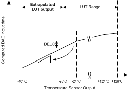 Figure 26. Temperature Sensor Output
Although the maximum output of the temperature sensor is 127.9375°C, the LUT index corresponding to 128°C (DEL38) is required for proper interpolation when the temperature is above 124°C.
The increments stored in the LUT are 4-bit unsigned values. This limits the maximum slope of the transfer function stored in the LUT to:

Given this slope limit imposed by the LUT structure, and the fact that the LUT input range is 156°C (from –28°C to 128°C ), the maximum output range of the LUT due to the temperature sensor input is 624 LSBs, for the given BASE value.
NOTE
The maximum span of 624 codes can reside anywhere within the 0 to 4095 code space of the 12-bit DAC input. The total input code to the DAC is the sum of the increments (Δs) and the 12-bit BASE value.
8.3.3 Analog Signal Path
The simplified schematic of one analog channel of the device is shown in Figure 27. The LMP92066 contains 2 such channels. The following sub-sections describe each of the individual blocks within a channel.
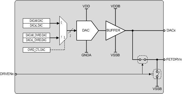 Figure 27. One Analog Channel Simplified Schematic
8.3.3.1 DAC
The DAC produces unipolar output voltage proportional to the 12-bit input code. The input code format is offset binary, where 0x000 represents minimum and the 0xFFF full-scale input. The input code is produced by the LUT/ALU and stored in the DACxM and DACxL read-only registers. The user can also insert the DAC input code via the DACxM_OVRD and DACxL_OVRD registers, and by setting the OVRD_CTL.DAC bit. The DAC is referenced to the internally generated 5 V.
The DAC transfer functions:

Where A is the Buffer Amplifier gain (see Buffer Amplifier) and DACIN is the 12-bit input code stored in either:

The LUT Input and Output Ranges describes the maximum output code span of the LUT, for the given base value. This also implies that when DACxM and DACxL registers are selected as the DAC inputs, the maximum VDACx output excursion over temperature is:

However, this limitation is lifted when using DACxM_OVRD and DACxL_OVRD registers as the DAC inputs. In this case the DAC input range is full 4096 codes, and the output spans 0 V to 5 V.
8.3.3.2 Buffer Amplifier
The buffer amplifier provides the low impedance drive for the potential generated by the DAC. The output of the amplifier is always available at the DACx output pin of the device. The buffer is designed to drive large capacitive loads, as high as 10 µF.
The structure of the Buffer is such that it can produce output voltages above or below GNDA potential. Both Buffer Amplifiers are biased from dedicated supply rails: VDDB and VSSB. The difference between the VDDB and VSSB is nominally 5 V, but the span can be above or below GNDA. The gain A of the Buffer Amplifier depends on the state of supply rails VDDB and VSSB.
When the span is above GNDA, or VDDB = 5 V and VSSB = 0 V, then the output buffer gain is A = 1. The net effect on the output of the analog processing chain is shown in Figure 28. The DAC input codes in the range of 0x000 to 0xFFF are mapped to the output voltage in the range of 0 V to 5 V.
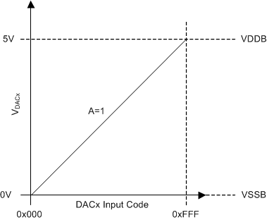 Figure 28. Output of Analog Processing Chain: Net Effect
If the span is below GNDA, or VDDB = 0 V and VSSB = –5 V, then the output buffer gain is A = –1. This configuration is depicted Figure 29. This results in effective mapping of the DAC input codes in the range of 0x000 to 0xFFF, to the output voltage range of 0 V to –5 V.
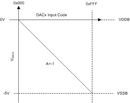 Figure 29. Common Mode Voltage Below GNDA,
 or VDDB = 0 V and VSSB = –5 V
NOTE
Both Buffer Amplifiers share the VDDB and VSSB rails. Therefore, both Buffers produce gain of A = 1, or both produce gain of A = –1.
The state of the VDDB and VSSB supplies, whether their span is above or below GNDA is indicated by the state of the DRV_STATUS.GAN bit, and can be read by the controller via the I2C interface.
8.3.3.3 Output On and Off Control
The LMP92066 facilitates rapid turnon and shutdown of the downstream devices. The FETDRVx outputs can be switched ON or OFF by the DRVENx input, independently of the I2C bus transactions. The FETDRVx pin is driven by the Buffer amplifier when the corresponding DRVENx input pin is asserted HIGH. Otherwise, the FETDRVx pin is connected to VSSB.
The control and switch design was optimized for minimum delay between the DRVENx input and the FETDRVx switching. The design also ensures that during the state transition there exists an instance when both switches at FETDRVx are open; that is, no possibility for the crow-bar current to flow from the Buffer output to VSSB.
The switches are assured to default to the state where FETDRVx output is connected to VSSB at power up, as long as logic 0 is present at the DRVENx input.
8.3.4 Memory
The internal memory of the device consists of 2 distinct areas: the user register set or operating memory and the EEPROM (non-volatile storage).
The operating memory registers provide the control over device functionality, report internal status of the device, and store the signal path data (LUT, temperature sensor output, etc). A section of operating memory, designated as a SCRATCH PAD, is available for arbitrary data storage. All operating memory locations are directly accessible to the user via the I2C bus.
The EEPROM is not directly accessible via the I2C bus. The EEPROM acquires its data via the transfer from the operating memory, upon user issued command.
Sections READ and WRITE Access, Access Control, LUT, NOTEPAD Storage, and EEPROM, and Figure 30 detail the internal memory functionality.
8.3.4.1 READ and WRITE Access
The operating memory consists of individually addressable bytes whose content can be accessed via a single I2C transaction. For 8-bit data, as soon as the I2C transfer is complete the transferred value takes effect.
The device also uses values longer that 8 bits — for example, with Temperature Sensor output, Temperature Sensor Override input, and the DAC input and Override registers are 12-bit values which require storage in 2 adjacent registers. For these values any access should start with the register containing the upper 4 bits, immediately followed by the access to the lower byte.
NOTE
It is the WRITE of the lower byte that results in the update of the 12-bit value. See Table 3.
Table 3. Block Writing
| I2C OPERATION | REGISTER | DATA | DESCRIPTION |
|---|---|---|---|
| WRITE | BLK_CNTL | 0x8F | Enable the BLOCK access and set the block length to 15. This transfer results in the immediate update of the BLK_CNTL register and immediate change of behavior of the I2C interface. |
| WRITE | TEMPM_OVRD | 0x08 | Write the upper nibble of the Temperature Sensor override value. This transaction does not result in the update of the TEMPM_OVRD register. The transferred value is placed on a queue awaiting the transfer of the lower byte. The output of the device is not affected. |
| WRITE | TEMPL_OVRD | 0x00 | Write the lower byte of the Temperature Sensor override value. This transaction results in the update of both the TEMPM_OVRD and TEMPL_OVRD registers. The output of the device changes accordingly with the new setting. |
8.3.4.2 Access Control
By default, all operating memory locations are open to READ access. The WRITE access is controlled by the Access Level setting. Increasing the Access Level, broadens the scope of the WRITE access. There are 3 access levels available to the user; see Access Control.
User can change the current Access Level by writing a “password” sequence to the ACC_CNTL register. The “password” sequences are 2 consecutive I2C byte transfers to the ACC_CNTL register. The data content of each 2 byte transfer is unique for each access level.
For example, to enter access level L2 perform the following 2 transfers:
Table 4. Memory Access Control
| I2C OPERATION | REGISTER | DATA | DESCRIPTION |
|---|---|---|---|
| WRITE | ACC_CNTL | 0xCD | First byte of the “password”. |
| WRITE | ACC_CNTL | 0xF0 | Second byte of the “password”. After this transfer is completed the access level is changed to L2. |
| READ | ACC_CNTL | 0x03 | Optional: Reading the ACC_CNTL serves as status report. The possible returned values are: 0x00 – access level L0 0x01 – access level L1 is activated 0x03 – access level L2 is activated (and due to nesting, L1 is also indicated) |
Table 5. EEPROM Access Levels
| ACCESS LEVEL | SCOPE |
|---|---|
| L0 | Default. User has READ access only to all locations in the operating memory. |
| L1 | User has READ access to all locations, and WRITE access to ADR_LK and BLK_CNTL registers. |
| L2 | User has READ and WRITE access to all operating memory locations. |
NOTE
The access levels are nested. This means that L1 access level also gives all L0 level functionality. L2 access level provides L1 and L0 functionality.
8.3.4.3 LUT, NOTEPAD Storage, and EEPROM
The LUT (its coefficients, BASE value, ALU control bits) and the NOTEPAD are stored in the operating memory block spanning addresses 0x40 through 0x7F. This space is directly accessible (READ and WIRITE) via the I2C bus.
There is an option to store the LUT and the NOTEPAD in the non-volatile memory, EEPROM. The move of data from the operating memory to the EEPROM (BURN) is initiated by WRITING a command byte to the EEPROM_CNTL register.
Upon power up the device automatically executes the TRANSFER of the EEPROM data to the operating memory. The user can also issue a command via the I2C bus to force the TRANSFER of data from the EEPROM to the operating memory.
Table 6. EEPROM Control
| TRANSFER/BURN | I2C OPERATION | REGISTER | DATA | COMMENT |
|---|---|---|---|---|
| TRANSFER | WRITE | EEPROM_CNTL | 0x4E | Transfer of data from the EEPROM to the operating memory. |
| BURN | WRITE | EEPROM_CNTL | 0xE4 | Transfer of data from the operating memory to the EEPROM. |
The READ of the EEPROM_CNTL register returns the status of the BURN or TRANSFER.
Table 7. Status of BURN or TRANSFER
| EEPROM_CNTL BIT FIELD | DESCRIPTION |
|---|---|
| RDYB | 0 - The TRANSFER or BURN has completed 1 – The TRANSFER or BURN is in progress |
| COR | 1 – A bit error was detected during the transfer from EEPROM to the operating memory. The error has been corrected and the data is valid. |
| UCOR | 1 – A bit error was detected during the transfer from EEPROM to operating memory. The error was not corrected. LUT data is compromised. |
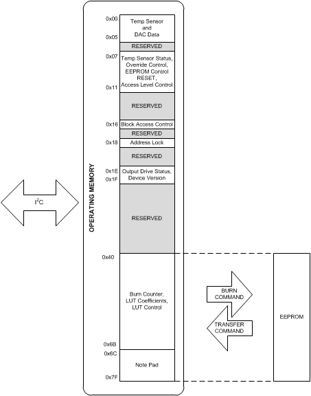 Figure 30. Memory-to-EEPROM Mapping
8.3.5 I2C Interface
I2C bus is used for communication between the Master (the digital supervisor; for example, the microcontroller) and the Slave (LMP92066). This interface provides the user full access to all Data, Status, and Control registers of the device.
LMP92066 supports Standard-mode and Fast-mode, 100 kbit/s and 400 kbit/s, respectively.
All transactions follow the format:
- Master begins all transactions by generating START condition.
- All transfers comprise 8-bit bytes.
- First byte following START must contain 7-bit Slave address.
- First byte is followed by a READ/WRITE bit.
- All subsequent bytes contain 8-bit data.
- By default, the device assumes 1-byte data transfers. Block access can be enabled via BLK_CNTL register, resulting in multi-byte transfers.
- Bit order within a byte is always MSB first
- ACK/NAK condition follows every byte transfer – this can be generated by either Master or the Slave depending on direction of data transfer.
- STOP condition generated by the MASTER terminates all transactions, and resets the I2C bus. LMP92066 resets its internal address pointer to 0x00.
8.3.5.1 Supported Data Transfer Formats
Table 8 lists all conditions defined by the I2C specification and supported by this device. All following bus descriptions refer to the symbols listed in Table 8.
Table 8. I2C Symbol Set
| CONDITION | SYMBOL | SOURCE | DESCRIPTION |
|---|---|---|---|
| START | S | Master | Begins all bus transactions |
| STOP | P | Master | Terminates all transations and resets bus |
| ACK (Acknowledge) | A | Master/Slave | Handshaking bit (LOW) |
| NAK (Not Acknowledge) | A | Master/Slave | Handshaking bit (HIGH) |
| READ | R | Master | Active HIGH bit that follows immediately after the slave address sequence. Indicates that the master is initiating the slave-to-master data transfer. |
| WRITE | W | Master | Active LOW bit that follows immediately after the slave address sequence. Indicates that the master is initiating the master-to-slave data transfer. |
| REPEATED START | Sr | Master | Generated by master, same function as the START condition (highlights the fact that STOP condition is not strictly necessary.) |
The single data byte transfers are shown in Figure 31 and Figure 32:
 Figure 31. Single-Byte WRITE Access Protocol
 Figure 32. Single-Byte READ Access Protocol
Block Access functionality is provided to minimize the transfer overhead of large data sets. By default the LMP92066 is ready to accept multi-byte transfers. Until the transaction is terminated by the STOP condition, the device will READ (WRITE) the subsequent memory locations.
The size of the contiguous block can be limited by the user. This functionality can be enabled by setting BLK_CNTL.EN bit. The 7-bit value of BLK_CNTL.SIZE=N sets the size of the contiguous memory block that can be accessed via the block transfer.
If the Master generates a block transfer that is larger than (BLK_CNTL.SIZE + 1), the internal register pointer wraps around to the First Register address and the access continue to subsequent memory locations. The examples of the block WRITE and READ transactions are shown below in Figure 33 and Figure 34:
 Figure 33. Block WRITE Access —
BLK_CNTL.EN = 1, BLK_CNTL.SIZE = N
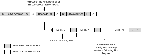 Figure 34. Block READ Access —
BLK_CNTL.EN = 1, BLK_CNTL.SIZE = N
8.3.5.2 Slave Address Selection
The I2C bus slave address is selected by installing shunts from A0 and A1 pins of the device to the VIO or GNDD rails. The device discerns between 3 possible options for each pin: shunt to VIO, shunt to GNDD, or left not connected (floating), for the total of 9 possible slave addresses.
The state of the A0 and A1 pins is tested after every occurrence of START condition on the I2C bus. However, the user has an option to LOCK the acquired address by setting the ADR_LK.EN bit. Once the address is locked, the device stores its Slave address internally and does not attempt to decode the address during subsequent I2C transactions. The address lock can be disabled by resetting ADR_LK.EN bit. The device resets the ADR_LK.EN upon power up.
Figure 35 and Figure 36 illustrate the operation of the address decoder circuit. The device internally attempts to pull up, and then pull down, the Ax pin while monitoring the voltage at that pin. If the shunts are installed, the weak pull-ups or pull-downs does not affect the voltage at the Ax pin; that is. the state is fixed by the shunt. If the Ax pin floats, then pull-up and pull-down change the voltage at that pin.
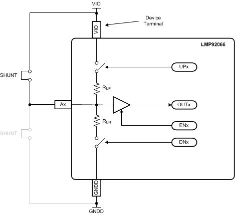 Figure 35. I2C Address Decoder - Simplified Diagram
The address decoder operates during 2nd through 4th cycles of the SCL. The decoding of the state of Ax pins is performed serially; that is, A0 is decoded first then A1. The functional diagram of the address decoder is shown in Figure 36.
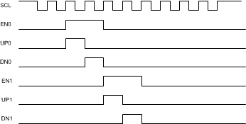 Figure 36. I2C Address Decoder - Functional Diagram
The interpretation of the OUTx values produced from the test phases is summarized in the following table. For example: if a shunt is present between Ax and VIO (first case in the table), both UPx phase and DNx phase result in OUTx being decoded as logical 1, unambiguously indicating the presence of the shunt to VIO, or HI state of Ax.
Table 9. Address Decoder Output
| TEST PHASE | DECODED Ax ↓ | ||
|---|---|---|---|
| UPx | DNx | ||
| SHUNT to VIO: OUTx → | 1 | 1 | HI |
| SHUNT to GNDD: OUTx → | 0 | 0 | LO |
| NO SHUNT: OUTx → | 1 | 0 | N.C. |
The mapping from the decoded Ax states to the I2C Slave address is shown in Table 10.
Table 10. Slave Address Space
| DEVICE PINS | I2C SLAVE ADDRESS | |
|---|---|---|
| A1 | A0 | [A6:A0] |
| LO | LO | 0111111 |
| LO | N.C. | 1000000 |
| LO | HI | 1000001 |
| N.C. | LO | 1000010 |
| N.C. | N.C. | 1000011 |
| N.C. | HI | 1000100 |
| HI | LO | 1000101 |
| HI | N.C. | 1000110 |
| HI | HI | 1000111 |
The Slave Address alignment within the first byte following the START condition is shown in Figure 37:
 Figure 37. Slave Address Alignment
8.4 Device Functional Modes
The numeric signal path is shown in Figure 38. The signal flow is generally from left to right: the system input is the temperature sensor, signal processing is done by the LUT/ALU, and the output is driven by the DACs - DAC detail is omitted as DACs provide a conversion from numeric domain to voltage domain only, and they do not affect the signal flow.
There are a number of multiplexers in the signal path which alter the data flow when their respective control bits are set. The multiplexer states, and thus modes of device operation, are described in further detail below.
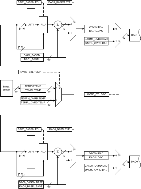 Figure 38. Modes of Operation
8.4.1 Default Operating Mode
This mode of operation is active upon power up. By default the OVRD_CTL.TEMP and OVRD_CTL.DAC are cleared. The temperature sensor continuously updates readings every 25 ms (registers: TEMPM, TEMPL). Each temperature sensor update triggers the ALU to re-calculate its output using the user defined coefficients stored in the LUT. The ALU output is passed on to the DACs (registers: DACxM, DACxL) which ultimately drive the VDACx outputs. All of the functionality described here occurs automatically, without intervention from the system controller, as long as the power is applied to the device supply pins: VDD, VIO, and VDDB.
8.4.2 Temperature Sensor Override
The temperature sensor output can be overridden by the externally supplied data. This capability may be used to verify the validity of the function stored in the LUT. The externally supplied data can act as the temperature sweep input and the output response due to temperature may be readily observed, without actually altering the temperature of the test setup.
This functionality is facilitated by the multiplexer that follows the temperature sensor, and user writable data registers TEMPM_OVRD and TEMPL_OVRD. TEMPM_OVRD[3:0] is the upper nibble of the temperature data. TEMPL_OVRD[7:0] is the lower byte of the temperature data. The multiplexer control signal is the OVRD_CTL.TEMP bit.
Table 11 shows an example of the I2C bus transfer sequence which results in externally supplied data indexing the LUT.
Table 11. I2C Bus Transfer Sequence:
Externally Supplied Data Indexing LUT
| I2C OPERATION | REGISTER | DATA | DESCRIPTION |
|---|---|---|---|
| WRITE | ACC_CNTL | 0xCD | First byte of the “password” |
| WRITE | ACC_CNTL | 0xF0 | Second byte of the “password”. After this transfer is completed the access level is changed to L2 |
| READ | ACC_CNTL | 0x03 | Optional: Reading the ACC_CNTL serves as status report. 0x03 – access level L2 is activated (and due to nesting, L1 is also indicated) |
| WRITE | TEMPM_OVRD | 0x01 | Writes 0x1 as the value of the top nibble of the 12-bit, twos complement, temperature value. After this transaction the TEMPM_OVRD register is not updated, yet. The update takes place only after the TEMPL_OVRD register is written. |
| WRITE | TEMPL_OVRD | 0x01 | Writes 0x01 into the lower byte of temperature value. After this transaction completes both TEMPM_OVRD and TEMPL_OVRD registers are updated. The 12-bit value in this example is 0x101 which corresponds to 16.0625°C |
| WRITE | OVRD_CTL | 0x01 | Sets the OVRD_CTL.TEMP bit. This causes the temperature stored in the TEMPM_OVRD and TEMPL_OVRD to index the LUT. |
| READ | TEMPM | 0x** | Optional: |
| READ | TEMPL | 0x** | Read the actual temperature reported by the temperature sensor. |
The temperature sensor override is cancelled by clearing the OVRD_CTL.TEMP bit.
NOTE
TEMPM_OVRD, TEMPL_OVRD and OVRD_CTL registers are in the volatile section of memory and are not backed by EEPROM. Upon power up these registers are cleared.
8.4.3 ALU Bypass
It may be desirable that the device produces a predetermined constant output level as soon as it is powered up. The ALU bypass mode does that. This mode is enabled by setting DACx_BASEM.BYP bit. Since DACx_BASEM.BYP is stored in the EEPROM, its value is automatically loaded into the operating memory at power up. If the stored value for DACx_BASEM.BYP is 1, upon power up the corresponding DAC output immediately produces an analog output equivalent of the BASE.
In this mode of operation the ALU is bypassed, and the BASE value of the LUT is presented at the input of the DAC. This is the result of DACx_BASEM.BYP, which controls the mux that follows the ALU in the signal path, being set. Therefore, the output of the device is constant over the operating temperature range of the device.
NOTE
Each channel has its own BYP bit, and its own BASE value.
8.4.4 DAC Input Override
The DAC inputs words can be directly written via the I2C interface. In this mode the LMP92066 is a dual 12-bit DAC. This functionality is facilitated by the multiplexers that precede the DACs, and user writable data registers DACxM_OVRD and DACxL_OVRD. DACxM_OVRD[3:0] is the upper nibble of the DAC input word. DACxL_OVRD[7:0] is the lower byte of the DAC input data.
The multiplexer control signal is the OVRD_CTL.DAC bit. This bit is shared by both channels; that is, both channels are either in the DAC input override mode, or both are in the default mode.
Table 12 shows the example of the I2C bus transfer sequence which results in externally supplied data being the source of input to the DACs.
Table 12. I2C Bus Transfer Sequence:
Externally Supplied Data Sourcing Input to DACs
| I2C OPERATION | REGISTER | DATA | DESCRIPTION |
|---|---|---|---|
| WRITE | ACC_CNTL | 0xCD | First byte of the “password” |
| WRITE | ACC_CNTL | 0xF0 | Second byte of the “password”. After this transfer is completed the access level is changed to L2 |
| READ | ACC_CNTL | 0x03 | Optional: Reading the ACC_CNTL serves as status report. 0x03 – access level L2 is activated (and due to nesting, L1 is also indicated) |
| WRITE | DAC0M_OVRD | 0x08 | Writes 0x8 as the value of the top nibble of the 12-bit, offset binary, DAC0 input value. After this transaction the DAC0M_OVRD register is not updated, yet. The update takes place only after the DAC0L_OVRD register is written. |
| WRITE | DAC0L_OVRD | 0x00 | Writes 0x00 into the lower byte of the DAC0 input value. After this transaction completes both DAC0M_OVRD and DAC0L_OVRD registers are updated. The 12-bit value in this example is 0x800. |
| WRITE | DAC1M_OVRD | 0x04 | Writes 0x4 as the value of the top nibble of the 12-bit, offset binary, DAC1 input value. After this transaction the DAC1M_OVRD register is not updated, yet. The update takes place only after the DAC1L_OVRD register is written. |
| WRITE | DAC1L_OVRD | 0x00 | Writes 0x00 into the lower byte of the DAC1 input value. After this transaction completes both DAC1M_OVRD and DAC1L_OVRD registers are updated. The 12-bit value in this example is 0x400. |
| WRITE | OVRD_CTL | 0x02 | Sets the OVRD_CTL.TEMP bit. This causes both multiplexers that precede the DACs to start routing the DACx_OVRD values to the inputs of their respective DACs. As a result the outputs of the device are: VDAC0 = 2.5 V, and VDAC1 = 1.25 V |
| READ | DAC0M | 0x** | Optional: |
| READ | DAC0L | 0x** | Read the values computed by the ALU. |
NOTE
The DAC Input Override and Temperature Sensor Override modes are mutually exclusive. The allowed values for OVRD_CTRL register are 0x00, 0x01 or 0x02.
NOTE
DACxM_OVRD, DACxL_OVRD and OVRD_CTL registers are in the volatile section of memory and are not backed by EEPROM. Upon power up these registers are cleared.
8.4.5 LDMOS and GaN Drives
The LDMOS mode and the GaN mode result from 2 possible biasing methods of the DAC output buffers – these were described in earlier sections of this data sheet.
The LDMOS mode is in effect when the VDDB and VSSB common mode is above GNDA. This mode is suitable for biasing of the LDMOS Power Amplifiers, since the output produced by the LMP92066 is in the 0 V to 5 V range. The GaN mode is in effect when the VDDB and VSSB common mode is below GNDA. This mode is suitable for biasing of the GaN type Power Amplifiers, as the output produced by the LMP92066 is in the 0V to –5V range.
8.5 Programming
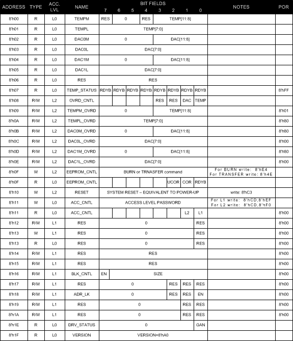
8.5.1 Temperature Sensor Output Data Access Registers
The temperature sensor produces a 12-bit output value, TEMP[11:0], which is stored in 2 adjacent registers: TEMPM and TEMPL.
The temperature sensor updates its output every 25 ms, nominally, but the exact instance of the update is unknown to the user. It is possible that the temperature sensor produces a new value between READ operations of TEMPM and TEMPL. Therefore, a synchronization mechanism was implemented, to assure that TEMPM and TEMPL values correspond to the same temperature sample. The coherence of the temperature sensor data is maintained if the READ sequence is: read TEMPM first, then TEMPL.
| ADDRESS | NAME | ACCESS TYPE | ACCESS LEVEL | BIT | FUNCTION | DESCRIPTION |
|---|---|---|---|---|---|---|
| 0x00 | TEMPM | R | L0 | 7 | RES | Reserved bit. The value may be reported as 0 or 1 |
| 6:5 | * | Reserved bit. Always reported as 0. |
||||
| 4 | RES | Reserved bit. The value may be reported as 0 or 1. |
||||
| 3:0 | TEMP[11:8] | 4-bit MSB nibble of the 12-bit Temperature Sensor output word. |
| ADDRESS | NAME | ACCESS TYPE | ACCESS LEVEL | BIT | FUNCTION | DESCRIPTION |
|---|---|---|---|---|---|---|
| 0x01 | TEMPL | R | L0 | 7:0 | TEMP[7:0] | 8-bit LSB byte of the 12-bit Temperature Sensor output word. |
8.5.2 DAC Input Data Registers
The 12-bit data produced by the LUT and ALU is stored in the DAC0M and DAC0L, and DAC1M and DAC1L pairs of registers. Unless overridden (see Override Control Register), the contents of these registers are presented at each DAC inputs.
In cases where the user wants to read the temperature sensor output and resulting DACxM or DACxL data, the following read order has to be maintained to assure the coherency of data: TEMPM, TEMPL, DAC0M, DAC0L, DAC1M, DAC1L.
Coherency of the TEMPM is still maintained, and TEMPL read is omitted in the sequence above.
| ADDRESS | NAME | ACCESS TYPE | ACCESS LEVEL | BIT | FUNCTION | DESCRIPTION |
|---|---|---|---|---|---|---|
| 0x02 | DAC0M | R | L0 | 7:4 | * | Reserved bit. Always report as 0. |
| 3:0 | DAC[11:8] | 4-bit MSB nibble of the 12-bit DAC0 input word. |
| ADDRESS | NAME | ACCESS TYPE | ACCESS LEVEL | BIT | FUNCTION | DESCRIPTION |
|---|---|---|---|---|---|---|
| 0x03 | DAC0L | R | L0 | 7:0 | DAC[7:0] | 8-bit LSB byte of the 12-bit Temperature Sensor output word. |
| ADDRESS | NAME | ACCESS TYPE | ACCESS LEVEL | BIT | FUNCTION | DESCRIPTION |
|---|---|---|---|---|---|---|
| 0x04 | DAC1M | R | L0 | 7:4 | * | Reserved bit. Always report as 0. |
| 3:0 | DAC[11:8] | 4-bit MSB nibble of the 12-bit DAC1 input word. |
| ADDRESS | NAME | ACCESS TYPE | ACCESS LEVEL | BIT | FUNCTION | DESCRIPTION |
|---|---|---|---|---|---|---|
| 0x05 | DAC1L | R | L0 | 7:0 | TEMP[7:0] | 8-bit LSB byte of the 12-bit DAC1 input word. |
8.5.3 Temperature Sensor Status Register
This register may contain non-zero values immediately after the device power up. Within 100 ms of the power up the TEMP_STATUS register clears, indicating the temperature sensor’s output is valid.
| ADDRESS | NAME | ACCESS TYPE | ACCESS LEVEL | BIT | FUNCTION | DESCRIPTION |
|---|---|---|---|---|---|---|
| 0x07 | TEMP_STATUS | R | L0 | 7:0 | RBYB | If RDYB=0x00, the Temperature Sensor is initialized and producing valid output. |
8.5.4 Override Control Register
Override functionality allows the user to insert external data into the signal path of the device. When TEMP override is enabled, the temperature sensor’s data is ignored, and the user-supplied data is used to index the LUT (TEMPM_OVRD and TEMPL_OVRD, below). When DAC override is enabled the LUT and ALU produced output is ignored, and both DAC0 and DAC1 use external data as their inputs (DAC0M_OVRD, DAC0L_OVRD and DAC1M_OVRD and DAC1L_OVRD described below).
NOTE
Only 3 OVRD_CNTL[2:0] settings are allowed: 0x0, 0x1, 0x2; simultaneous DAC and TEMP override is not allowed.
| ADDRESS | NAME | ACCESS TYPE | ACCESS LEVEL | BIT | FUNCTION | DESCRIPTION |
|---|---|---|---|---|---|---|
| 0x08 | OVRD_CNTL | R/W | L2 | 7:4 | * | Reserved bit. Always WRITE 0 |
| 3 | RES | Reserved bit. Always WRITE 0 | ||||
| 2 | RES | Reserved bit. Always WRITE 0 | ||||
| 1 | DAC | DAC override enable bit: 0: DAC input generated by LUT 1: DAC input is supplied from user accessible registers DACxy_OVRD. |
||||
| 0 | TEMP | DAC override enable bit: 0: DAC input generated by LUT 1: DAC input is supplied from user accesible registers TEMPy_OVRD. |
8.5.5 Override Data Registers
These registers hold the externally supplied data to be inserted into the signal path of the device (see OVRD_CNTL).
NOTE
Since override data are 12-bit words stored in 2 adjacent registers, it is the writing of the lower byte that makes the new value take effect.
| ADDRESS | NAME | ACCESS TYPE | ACCESS LEVEL | BIT | FUNCTION | DESCRIPTION |
|---|---|---|---|---|---|---|
| 0x09 | TEMPM_OVRD | R/W | L2 | 7:4 | * | Reserved bit. Always report as 0. |
| 3:0 | TEMP[11:8] | 4-bit MSB nibble of the 12-bit Temperature Sensor override input word. |
| ADDRESS | NAME | ACCESS TYPE | ACCESS LEVEL | BIT | FUNCTION | DESCRIPTION |
|---|---|---|---|---|---|---|
| 0x0A | TEMPL_OVRD | R/W | L2 | 7:0 | TEMP[7:0] | 8-bit LSB byte of the 12-bit Temperature Sensor output word. |
| ADDRESS | NAME | ACCESS TYPE | ACCESS LEVEL | BIT | FUNCTION | DESCRIPTION |
|---|---|---|---|---|---|---|
| 0x0B | DAC0M_OVRD | R/W | L2 | 7:4 | * | Reserved bit. Always report as 0. |
| 3:0 | DAC[11:8] | 4-bit MSB nibble of the 12-bit DAC0 input override word. |
| ADDRESS | NAME | ACCESS TYPE | ACCESS LEVEL | BIT | FUNCTION | DESCRIPTION |
|---|---|---|---|---|---|---|
| 0x0C | DAC0L_OVRD | R/W | L2 | 7:0 | DAC[7:0] | 8-bit LSB byte of the 12-bit DAC0 input override word. |
| ADDRESS | NAME | ACCESS TYPE | ACCESS LEVEL | BIT | FUNCTION | DESCRIPTION |
|---|---|---|---|---|---|---|
| 0x0D | DAC1M_OVRD | R/W | L2 | 7:4 | * | Reserved bit. Always report as 0. |
| 3:0 | DAC[11:8] | 4-bit MSB nibble of the 12-bit DAC1 input override word. |
| ADDRESS | NAME | ACCESS TYPE | ACCESS LEVEL | BIT | FUNCTION | DESCRIPTION |
|---|---|---|---|---|---|---|
| 0x0E | DAC1L_OVRD | R/W | L2 | 7:0 | DAC[7:0] | 8-bit LSB byte of the 12-bit DAC1 input override word. |
8.5.6 EEPROM Control Register
Writing a command byte results in either the EEPROM BURN (the commitment of a section of operating memory to non-volatile storage), or the TRANSFER (recall of the data in the non-volatile storage to the operating memory.
Reading this register yields status information.
NOTE
UCOR and COR bits are updated only by the TRANSFER command.
| ADDRESS | NAME | ACCESS TYPE | ACCESS LEVEL | BIT | FUNCTION | DESCRIPTION |
|---|---|---|---|---|---|---|
| 0x0F | EEPROM_CNTL | W | L2 | 7:0 | * | Instruction to BURN EEPROM or TRANSFER EEPROM content to operating memory: 0xE4: BURN EEPROM. 0x4E: TRANSFER data from EEPROM to operating memory. |
| R | L0 | 7:3 | * | Reserved bit. | ||
| 2 | UCOR | 1: More than one bit error was detected during the TRANSFER, and correction was not possible. 0: No uncorrected errors were detected during the TRANSFER. |
||||
| 1 | COR | 1: A bit error was detected and corrected during the TRANSFER. 0: No errors detected during the TRANSFER. |
||||
| 0 | RDYB | 1: BURN or TRANSFER in progress. 0: BURN or TRANSFER completed. |
8.5.7 Software RESET Register
Has the same effect as the power-on reset.
| ADDRESS | NAME | ACCESS TYPE | ACCESS LEVEL | BIT | FUNCTION | DESCRIPTION |
|---|---|---|---|---|---|---|
| 0x10 | RESET | W | L2 | 7:0 | DAC[7:0] | WRITE 0xC3 to reset the deice to the power-up default state. |
8.5.8 Access Control Register
Changing the Access Level requires writing the 2-byte password sequence. Reading this register yields status information.
| ADDRESS | NAME | ACCESS TYPE | ACCESS LEVEL | BIT | FUNCTION | DESCRIPTION |
|---|---|---|---|---|---|---|
| 0x11 | ACC_CNTL | W | L0 | 7:0 | PSWD | WRITE 2-byte password to change access level: 0xCD, 0xEF: Access Level L1. 0xCD, 0xF0: Access Level L2. |
| R | L0 | 7:2 | * | * | ||
| 1 | * | 1: Access Level L2 is enabled. 0: L2 not enabled. |
||||
| 0 | RES | 1: Access Level L1 is enabled. 0: L1 not enabled. |
8.5.9 Block I2C Access Control Register
The I2C master may request a continuous transfer of data from or to the slave. By default, the slave continues advancing its internal register pointer to the end of the internal register space, and then wrap back to address 0x00 and continue on.
BLK_CNTL allows to limit the size of the contiguous memory accessed continuously.
| ADDRESS | NAME | ACCESS TYPE | ACCESS LEVEL | BIT | FUNCTION | DESCRIPTION |
|---|---|---|---|---|---|---|
| 0x16 | BLK_CNTL | R/W | L1 | 7 | EN | Enable the control of the I2C access block size: 1: Enabled. 0: Block size control is disabled. |
| 6:0 | * | 7-bit SIZE of the I2C access block. The continuous I2C transaction accesses SIZE+1 memory locations, and then wrap back to the starting address. |
8.5.10 I2C Address LOCK Register
Allows the device to LOCK its own I2C slave address. Once the slave address is locked, the device does not attempt to decode the state of A0 and A1 address setting pins on subsequent transactions.
| ADDRESS | NAME | ACCESS TYPE | ACCESS LEVEL | BIT | FUNCTION | DESCRIPTION |
|---|---|---|---|---|---|---|
| 0x18 | ADR_LK | R/W | L1 | 7:3 | * | Always set to 0 |
| 2 | RES | Reserved bit. Always write 0. | ||||
| 1 | RES | Reserved bit. Always write 0. | ||||
| 0 | EN | 1: Lock the slave address 0: Slave address is not locked. Device decodes state of A1 and A0 after every START condition of the I2C bus. |
NOTE
The locked address is the one present at the A[1:0] pins during the I2C transaction that follows the ADR_LK command.
8.5.11 Output Drive Supply Status Register
The device output stage can operate in either LDMOS or GaN modes. The mode is determined by the potential applied to the VDDB and VSSB supply pins.
The device monitors the VDDB and VSSB supplies, and reports the mode of operation via the GaN status bit.
| ADDRESS | NAME | ACCESS TYPE | ACCESS LEVEL | BIT | FUNCTION | DESCRIPTION |
|---|---|---|---|---|---|---|
| 0x1E | DRV-STATUS | R | L0 | 7:1 | * | Reserved. Always reports 0 |
| 0 | GAN | 1: GaN mode supply rails detected; that is, VDDB = GNDA, VSSB = –5V. 0: LDMOS mode supply rails detected; that is, VDDB = +5V, VSSB = GNDA. |
8.5.12 Device Version Register
Factory set value.
| ADDRESS | NAME | ACCESS TYPE | ACCESS LEVEL | BIT | FUNCTION | DESCRIPTION |
|---|---|---|---|---|---|---|
| 0x1F | VERSION | R | L0 | 7:0 | VERSION | 8-bit device revision number. |
8.5.13 EEPROM Burn Counter
The value is incremented automatically at the start of BURN sequence.
This data is transferred automatically from the EEPROM to operating memory upon power up.
| ADDRESS | NAME | ACCESS TYPE | ACCESS LEVEL | BIT | FUNCTION | DESCRIPTION |
|---|---|---|---|---|---|---|
| 0x40 | BURN_CT | R | L0 | 7:0 | COUNT | 8-bit EEPROM BURN counter. |
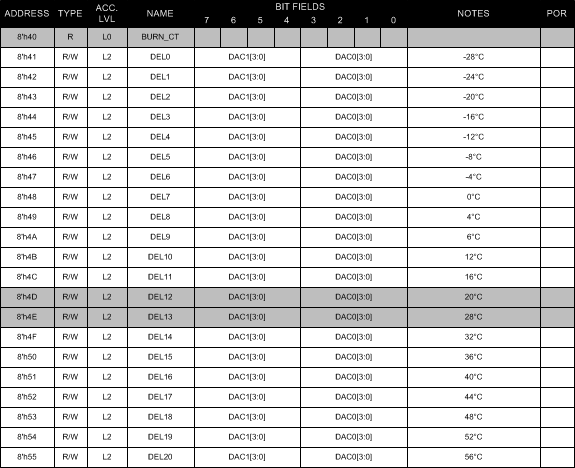
8.5.14 LUT Coefficient Registers
This data is transferred to the EEPROM when a BURN command sequence is issued.
This data is transferred automatically from the EEPROM to operating memory upon power up or after a software reset.
NOTE
The LUT values are stored at locations corresponding to 4°C increments from –28°C to 128°C. There is no increment corresponding to 24°C because this temperature is a BASELINE, and the corresponding LUT value is 12-bit BASE (see Look-Up-Table (LUT) and Arithmetic-Logic Unit (ALU) ).
| ADDRESS | NAME | ACCESS TYPE | ACCESS LEVEL | BIT | FUNCTION | DESCRIPTION |
|---|---|---|---|---|---|---|
| 0x41 | DEL0 | R/W | L2 | 7:4 | DAC1[3:0] | 4-bit LUT1 entry |
| ↓ | ↓ | |||||
| 0x4D | DEL12 (20°C) | |||||
| 0x4E | DEL13 (28°C) | 3:0 | DAC0[3:0] | 4-bit LUT0 entry | ||
| ↓ | ↓ | |||||
| 0x67 | DEL38 (128°C) |
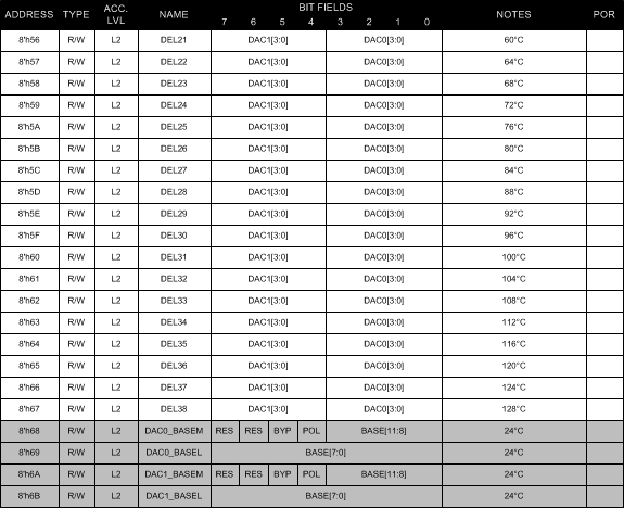
8.5.15 LUT Control Registers
This data is transferred to the EEPROM when a BURN command sequence is issued.
This data is transferred automatically from the EEPROM to operating memory upon power up.
| ADDRESS | NAME | ACCESS TYPE | ACCESS LEVEL | BIT | FUNCTION | DESCRIPTION |
|---|---|---|---|---|---|---|
| 0x68 | DAC0_BASEM | R/W | L2 | 7 | RES | Reserved bit. Always write 0. |
| 6 | RES | Reserved bit. Always reported as 0. | ||||
| 5 | BYP | ALU bypass control: 1: Bypass ALU. Send BASE value to DAC0. 0: ALU output sent to DAC0. |
||||
| 4 | POL | LUT increment polarity control: 1: All LUT values are treated as negatives. This realizes a monotonically decreasing LUT0 transfer function. 0: All LUT values are treated as positive numbers. This realizes a monotonically increasing LUT0 transfer function. |
||||
| 3:0 | BASE[11:8] | 4-bit MSB nibble of the 12-bit LUT0 BASE value (LUT0 output at +24°C). |
| ADDRESS | NAME | ACCESS TYPE | ACCESS LEVEL | BIT | FUNCTION | DESCRIPTION |
|---|---|---|---|---|---|---|
| 0x69 | DAC0_BASEL | R | L2 | 7:0 | BASE[7:0] | 8-bit LSB byte of the 12-bit BASE value (LUT0 output at +24°C). |
| ADDRESS | NAME | ACCESS TYPE | ACCESS LEVEL | BIT | FUNCTION | DESCRIPTION |
|---|---|---|---|---|---|---|
| 0x6A | DAC1_BASEM | R/W | L2 | 7 | RES | Reserved bit. Always write 0. |
| 6 | RES | Reserved bit. Always reported as 0. | ||||
| 5 | BYP | ALU bypass control: 1: Bypass ALU. Send BASE value to DAC1. 0: ALU output sent to DAC1. |
||||
| 4 | POL | LUT increment polarity control: 1: All LUT values are treated as negatives. This realizes a monotonically decreasing LUT1 transfer function. 0: All LUT values are treated as positive numbers. This realizes a monotonically increasing LUT1 transfer function. |
||||
| 3:0 | BASE[11:8] | 4-bit MSB nibble of the 12-bit LUT1 BASE value (LUT0 output at +24°C). |
| ADDRESS | NAME | ACCESS TYPE | ACCESS LEVEL | BIT | FUNCTION | DESCRIPTION |
|---|---|---|---|---|---|---|
| 0x6B | DAC1_BASEL | R | L2 | 7:0 | BASE[7:0] | 8-bit LSB byte of the 12-bit BASE value (LUT1 output at +24°C). |
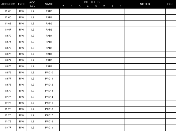
8.5.16 Notepad Registers
20 bytes of memory for arbitrary data storage. This data does not affect the operation of the device. This data is transferred to the EEPROM when BURN command sequence is issued.
This data is transferred automatically from the EEPROM to operating memory upon power up.
| ADDRESS | NAME | ACCESS TYPE | ACCESS LEVEL | BIT | FUNCTION | DESCRIPTION |
|---|---|---|---|---|---|---|
| 0x6C | PAD0 | R/W | L2 | 7:0 | * | 20 bytes of memory for arbitrary data storage. This data does not affect the operation of the device. This data is transferred to the EEPROM when BURN command sequence is issued via I2C transaction. |
| ↓ | ↓ | |||||
| 0x7F | PAD19 |
8.6 Register Map
