SNAS744B July   2017  – March 2018 LMS3655

PRODUCTION DATA.  

  1. Features
  2. Applications
  3. Description
    1.     Device Images
      1.      Typical Application Circuit
      2.      LMS3655 Efficiency: VOUT = 5 V
  4. Revision History
  5. Device Comparison Table
  6. Pin Configuration and Functions
    1.     Pin Functions
  7. Specifications
    1. 7.1 Absolute Maximum Ratings
    2. 7.2 ESD Ratings
    3. 7.3 Recommended Operating Conditions
    4. 7.4 Thermal Information
    5. 7.5 Thermal Information (for Device Mounted on PCB)
    6. 7.6 Electrical Characteristics
    7. 7.7 System Characteristics
    8. 7.8 Timing Requirements
    9. 7.9 Typical Characteristics
  8. Detailed Description
    1. 8.1 Overview
    2. 8.2 Functional Block Diagram
      1. 8.2.1 Control Scheme
    3. 8.3 Feature Description
      1. 8.3.1 RESET Flag Output
      2. 8.3.2 Enable and Start-Up
      3. 8.3.3 Soft-Start Function
      4. 8.3.4 Current Limit
      5. 8.3.5 Hiccup Mode
      6. 8.3.6 Synchronizing Input
      7. 8.3.7 Undervoltage Lockout (UVLO) and Thermal Shutdown (TSD)
      8. 8.3.8 Input Supply Current
    4. 8.4 Device Functional Modes
      1. 8.4.1 AUTO Mode
      2. 8.4.2 FPWM Mode
      3. 8.4.3 Dropout
      4. 8.4.4 Spread-Spectrum Operation
  9. Application and Implementation
    1. 9.1 Application Information
    2. 9.2 Typical Applications
      1. 9.2.1 General Application
        1. 9.2.1.1 Design Requirements
        2. 9.2.1.2 Detailed Design Procedure
          1. 9.2.1.2.1 External Components Selection
            1. 9.2.1.2.1.1 Input Capacitors
            2. 9.2.1.2.1.2 Output Inductors and Capacitors
              1. 9.2.1.2.1.2.1 Inductor Selection
              2. 9.2.1.2.1.2.2 Output Capacitor Selection
          2. 9.2.1.2.2 FB for Adjustable Output
          3. 9.2.1.2.3 VCC
          4. 9.2.1.2.4 BIAS
          5. 9.2.1.2.5 CBOOT
          6. 9.2.1.2.6 Maximum Ambient Temperature
        3. 9.2.1.3 Application Curves
      2. 9.2.2 Adjustable 5-V Output
        1. 9.2.2.1 Design Requirements
        2. 9.2.2.2 Detailed Design Procedure
        3. 9.2.2.3 Application Curves
      3. 9.2.3 Adjustable 3.3-V Output
        1. 9.2.3.1 Design Requirements
        2. 9.2.3.2 Detailed Design Procedure
        3. 9.2.3.3 Application Curves
      4. 9.2.4 6-V Adjustable Output
        1. 9.2.4.1 Design Requirements
        2. 9.2.4.2 Detailed Design Procedure
        3. 9.2.4.3 Application Curves
    3. 9.3 Do's and Don't's
  10. 10Power Supply Recommendations
  11. 11Layout
    1. 11.1 Layout Guidelines
    2. 11.2 Layout Example
  12. 12Device and Documentation Support
    1. 12.1 Device Support
      1. 12.1.1 Third-Party Products Disclaimer
    2. 12.2 Documentation Support
      1. 12.2.1 Related Documentation
    3. 12.3 Receiving Notification of Documentation Updates
    4. 12.4 Community Resources
    5. 12.5 Trademarks
    6. 12.6 Electrostatic Discharge Caution
    7. 12.7 Glossary
  13. 13Mechanical, Packaging, and Orderable Information

Package Options

Mechanical Data (Package|Pins)
Thermal pad, mechanical data (Package|Pins)
Orderable Information

Application Curves

The following characteristics apply only to the circuit of Adjustable 5-V Output. These parameters are not tested and represent typical performance only. Unless otherwise stated, the following conditions apply: VIN = 12 V, TA = 25°C. For the purpose of offering more information to the designer, information for the application with FPWM pin high (FPWM mode) and FPWM pin low (AUTO mode) is included, although the schematic shows the application running specifically in FPWM mode. The mode is specified under each following graph.
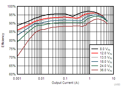
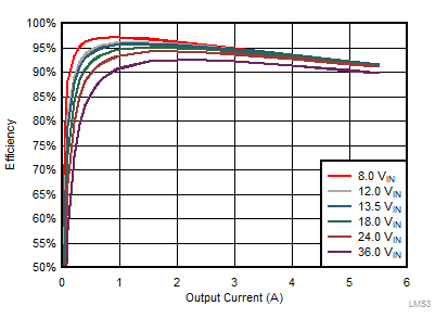
LMS3655 LMS3635-55-tc09-efficiency-auto-snas701.gif
VOUT = 5 V AUTO
Figure 24. Efficiency
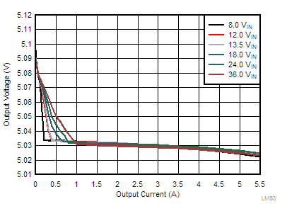
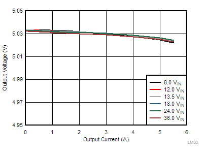
LMS3655 LMS3635-55-tc11-load-and-line-regulation-auto-snas701.gif
VOUT = 5 V AUTO
Figure 26. Load and Line Regulation
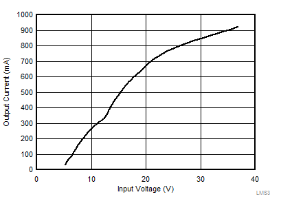
LMS3655 LMS3635-55-tc14-load-current-for-pfm-to-pwm-transition-snas701.gif
VOUT = 5 V
Figure 28. Load Current for PFM-to-PWM Transition
LMS3655 LMS3635-55-tc16-dropout-for-less-than-330khz-snas701.gif
VOUT = 5 V
Figure 30. Dropout for ≥ 330 kHz
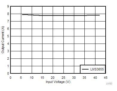
LMS3655 LMS3655-tc19-output-current-level-limit-before-over-current-protection-snas744.gif
VOUT = 5 V L = 10 µH
Figure 32. Output Current Level Limit Before Overcurrent Protection
LMS3655 LT-13p5_vin_5vout_fpwm.png
FPWM VOUT = 5 V L = 10 µH
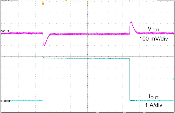
COUT = 170 µF IOUT = 0 A to 3.5 A TR = TF = 1 µs
Figure 34. Load Transient
LMS3655 LMS3635-55-tc10-efficiency-fpwm-snas701.gif
VOUT = 5 V FPWM
Figure 25. Efficiency
LMS3655 LMS3635-55-tc12-load-and-line-regulation-fpwm-snas701.gif
VOUT = 5 V FPWM
Figure 27. Load and Line Regulation
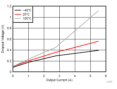
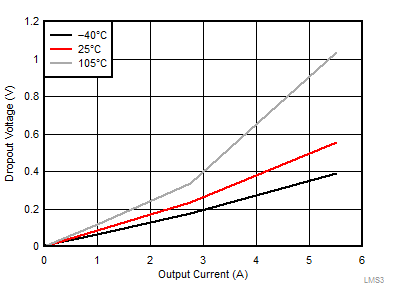
LMS3655 LMS3635-55-tc15-dropout-for-neg-3-percent-regulation-snas701.gif
VOUT = 5 V
Figure 29. Dropout for –3% Regulation
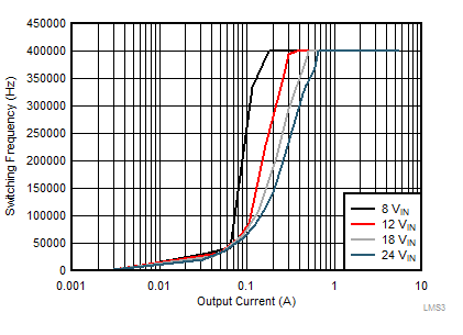
LMS3655 LMS3635-55-tc17-switching-frequency-vs-load-current-snas701.gif
VOUT = 5 V AUTO
Figure 31. Switching Frequency vs Load Current
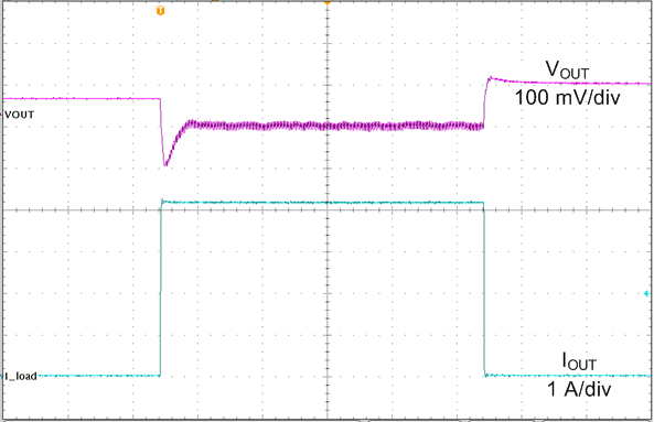
LMS3655 LT-13p5_vin_5vout_auto.png
AUTO VOUT = 5 V L = 10 µH
COUT = 170 µF IOUT = 10 mA to 3.5 A TR = TF = 1 µs
Figure 33. Load Transients