SNOS487F May 2004 – December 2016 LMS8117A
PRODUCTION DATA.
- 1 Features
- 2 Applications
- 3 Description
- 4 Revision History
- 5 Pin Configuration and Functions
- 6 Specifications
- 7 Detailed Description
- 8 Application and Implementation
- 9 Power Supply Recommendations
- 10Layout
- 11Device and Documentation Support
- 12Mechanical, Packaging, and Orderable Information
Package Options
Mechanical Data (Package|Pins)
Thermal pad, mechanical data (Package|Pins)
Orderable Information
1 Features
- Available in 1.8-V, 3.3-V, and Adjustable Versions
- Space-Saving SOT-223 and TO-252 Packages
- Current Limiting and Thermal Protection
- Output Current: 1 A
- Temperature Range: 0°C to 125°C
- Line Regulation: 0.2% (Maximum)
- Load Regulation: 0.4% (Maximum)
2 Applications
- Post Regulator for Switching DC-DC Converters
- High Efficiency Linear Regulators
- Battery Chargers
- Battery-Powered Instrumentation
3 Description
The LMS8117A device is a series of low-dropout voltage regulators with a dropout of 1.2 V at 1 A of load current. The device has the same pinout as the LM317.
The LMS8117A is available in an adjustable version, which can set the output voltage from 1.27 V to
13.8 V with only two external resistors. In addition, the device is also available in two fixed voltages,
1.8 V and 3.3 V.
The LMS8117A offers current limiting and thermal shutdown. The device circuit includes a Zener trimmed band-gap reference to assure output voltage accuracy to within ±1%.
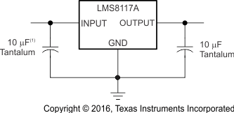
The LMS8117A is available in SOT-223 and TO-252 D-PAK packages. A 10-µF (minimum) tantalum capacitor is required at the output to improve the transient response and stability.
Device Information(1)
| PART NUMBER | PACKAGE | BODY SIZE (NOM) |
|---|---|---|
| LMS8117A | SOT-223 (4) | 3.50 mm × 6.50 mm |
| TO-252 (3) | 6.10 mm × 6.58 mm |
- For all available packages, see the orderable addendum at the end of the data sheet.
Functional Block Diagram
