SNOS998I February 2002 – October 2015 LMV761 , LMV762 , LMV762Q-Q1
PRODUCTION DATA.
- 1 Features
- 2 Applications
- 3 Description
- 4 Revision History
- 5 Pin Configuration and Functions
-
6 Specifications
- 6.1 Absolute Maximum Ratings
- 6.2 ESD Ratings: LMV761, LMV762
- 6.3 ESD Ratings: LMV762Q-Q1
- 6.4 Recommended Operating Conditions
- 6.5 Thermal Information
- 6.6 2.7-V Electrical Characteristics
- 6.7 5-V Electrical Characteristics
- 6.8 2-V Switching Characteristics
- 6.9 5-V Switching Characteristics
- 6.10 Typical Characteristics
- 7 Detailed Description
- 8 Application and Implementation
- 9 Power Supply Recommendations
- 10Layout
- 11Device and Documentation Support
- 12Mechanical, Packaging, and Orderable Information
Package Options
Mechanical Data (Package|Pins)
Thermal pad, mechanical data (Package|Pins)
Orderable Information
8 Application and Implementation
NOTE
Information in the following applications sections is not part of the TI component specification, and TI does not warrant its accuracy or completeness. TI’s customers are responsible for determining suitability of components for their purposes. Customers should validate and test their design implementation to confirm system functionality.
8.1 Application Information
The LMV76x are single-supply comparators with 120 ns of propagation delay and 300 µA of supply current.
8.2 Typical Application
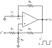
A typical application for a LMV76x comparator is a programmable square-wave oscillator.
 Figure 23. Square-Wave Oscillator
8.2.1 Design Requirements
The circuit in Figure 23 generates a square wave whose period is set by the RC time constant of the capacitor C1 and resistor R4. V+ = 5 V unless otherwise specified.
8.2.2 Detailed Design Procedure
The maximum frequency is limited by the large signal propagation delay of the comparator and by the capacitive loading at the output, which limits the output slew rate.
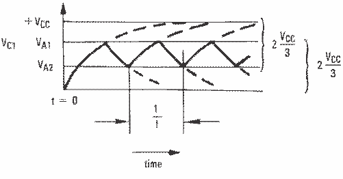
 Figure 24. Square-Wave Oscillator Timing Thresholds
Consider the output of Figure 23 is high to analyze the circuit. That implies that the inverted input (VC) is lower than the noninverting input (VA). This causes the C1 to be charged through R4, and the voltage VC increases until it is equal to the noninverting input. The value of VA at this point is calculated by Equation 4:

If R1 = R2 = R3, then VA1 = 2 VCC / 3
At this point the comparator switches pulling down the output to the negative rail. The value of VA at this point is calculated by Equation 5:

If R1 = R2 = R3, then VA2 = VCC / 3.
The capacitor C1 now discharges through R4, and the voltage VC decreases until it is equal to VA2, at which point the comparator switches again, bringing it back to the initial stage. The time period is equal to twice the time it takes to discharge C1 from 2 VCC / 3 to VCC / 3, which is given by R4C1 × ln2. Hence, the formula for the frequency is calculated by Equation 6:
8.2.3 Application Curve
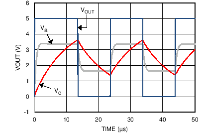
Figure Figure 25 shows the simulated results of an oscillator using the following values:
- R1 = R2 = R3 = R4 = 100 kΩ
- C1 = 100 pF, CL = 20 pF
- V+ = 5 V, V– = GND
- CSTRAY (not shown) from Va to GND = 10 pF
 Figure 25. Square-Wave Oscillator Output Waveform