SNOS998I February 2002 – October 2015 LMV761 , LMV762 , LMV762Q-Q1
PRODUCTION DATA.
- 1 Features
- 2 Applications
- 3 Description
- 4 Revision History
- 5 Pin Configuration and Functions
-
6 Specifications
- 6.1 Absolute Maximum Ratings
- 6.2 ESD Ratings: LMV761, LMV762
- 6.3 ESD Ratings: LMV762Q-Q1
- 6.4 Recommended Operating Conditions
- 6.5 Thermal Information
- 6.6 2.7-V Electrical Characteristics
- 6.7 5-V Electrical Characteristics
- 6.8 2-V Switching Characteristics
- 6.9 5-V Switching Characteristics
- 6.10 Typical Characteristics
- 7 Detailed Description
- 8 Application and Implementation
- 9 Power Supply Recommendations
- 10Layout
- 11Device and Documentation Support
- 12Mechanical, Packaging, and Orderable Information
Package Options
Mechanical Data (Package|Pins)
Thermal pad, mechanical data (Package|Pins)
Orderable Information
7 Detailed Description
7.1 Overview
The LMV76x family of precision comparators is available in a variety of packages and is ideal for portable and battery-operated electronics.
To minimize external components, the LMV76x family features a push-pull output stage where the output levels are power-supply determined. In addition, the LMV761 (single) features an active-low shutdown pin that can be used to disable the device and reduce the supply current.
7.2 Functional Block Diagram
7.3 Feature Description
7.3.1 Basic Comparator
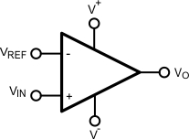
A basic comparator circuit is used to convert analog input signals to digital output signals. The comparator compares an input voltage (VIN) at the noninverting input to the reference voltage (VREF) at the inverting pin. If VIN is less than VREF the output (VO) is low (VOL). However, if VIN is greater than VREF, the output voltage (VO) is high (VOH).
 Figure 19. Basic Comparator Without Hysteresis
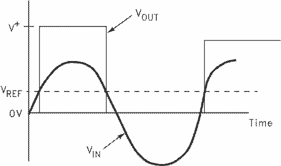 Figure 20. Basic Comparator
7.3.2 Hysteresis
The basic comparator configuration may oscillate or produce a noisy output if the applied differential input is near the input offset voltage of the comparator, which tends to occur when the voltage on one input is equal or very close to the other input voltage. Adding hysteresis can prevent this problem. Hysteresis creates two switching thresholds (one for the rising input voltage and the other for the falling input voltage). Hysteresis is the voltage difference between the two switching thresholds. When both inputs are nearly equal, hysteresis causes one input to effectively move quickly past the other. Thus, moving the input out of the region in which oscillation may occur.
Hysteresis can easily be added to a comparator in a noninverting configuration with two resistors and positive feedback Figure 22. The output will switch from low to high when VIN rises up to VIN1, where VIN1 is calculated by Equation 1:
The output will switch from high to low when VIN falls to VIN2, where VIN2 is calculated by Equation 2:
The Hysteresis is the difference between VIN1 and VIN2, as calculated by Equation 3:
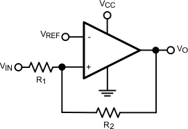 Figure 21. Basic Comparator With Hysteresis
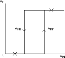 Figure 22. Noninverting Comparator Configuration
7.3.3 Input
The LMV76x devices have near-zero input bias current, which allows very high resistance circuits to be used without any concern for matching input resistances. This near-zero input bias also allows the use of very small capacitors in R-C type timing circuits. This reduces the cost of the capacitors and amount of board space used.
7.4 Device Functional Modes
7.4.1 Shutdown Mode
The LMV761 features a low-power shutdown pin that is activated by driving SD low. In shutdown mode, the output is in a high-impedance state, supply current is reduced to 20 nA and the comparator is disabled. Driving SD high will turn the comparator on. The SD pin must not be left unconnected due to the fact that it is a high-impedance input. When left unconnected, the output will be at an unknown voltage. Do not three-state the SD pin.
The maximum input voltage for SD is 5.5 V referred to ground and is not limited by VCC. This allows the use of
5-V logic to drive SD while VCC operates at a lower voltage, such as 3 V. The logic threshold limits for SD are proportional to VCC.