SNVSAG0A November 2016 – February 2017 LP5922
PRODUCTION DATA.
- 1 Features
- 2 Applications
- 3 Description
- 4 Revision History
- 5 Pin Configuration and Functions
- 6 Specifications
- 7 Detailed Description
-
8 Applications and Implementation
- 8.1 Application Information
- 8.2
Typical Application
- 8.2.1 Design Requirements
- 8.2.2
Detailed Design Procedure
- 8.2.2.1 Custom Design With WEBENCH® Tools
- 8.2.2.2 External Capacitors
- 8.2.2.3 Input Capacitor, CIN
- 8.2.2.4 Output Capacitor, COUT
- 8.2.2.5 Soft-Start and Noise-Reduction Capacitor, CSS/NR
- 8.2.2.6 Feed-Forward Capacitor, CFF
- 8.2.2.7 No-Load Stability
- 8.2.2.8 Power Dissipation
- 8.2.2.9 Estimating Junction Temperature
- 8.2.2.10 Recommended Continuous Operating Area
- 8.2.3 Application Curves
- 9 Power Supply Recommendations
- 10Layout
- 11Device and Documentation Support
- 12Mechanical, Packaging, and Orderable Information
Package Options
Mechanical Data (Package|Pins)
- DSC|10
Thermal pad, mechanical data (Package|Pins)
- DSC|10
Orderable Information
1 Features
- Wide Input Voltage Range: 1.3 V to 6 V
- Low VIN Voltage Without Extra Bias Voltage
- Adjustable Output Voltage: 0.5 V to 5 V
- Low Dropout: 200 mV at 2-A Load
- Low Output Voltage Noise: 25 μVRMS
- Output Current: 2 A
- –40˚C to +125°C Operating Junction Temperature
- Programmable Soft Start Limits Inrush Current
- 3-mm × 3-mm × 0.75-mm 10-Pin WSON Package
- Thermal-Overload and Short-Circuit Protection
- Output Voltage Tolerance: ±1.5%
- Shutdown Supply Current : 0.1 μA
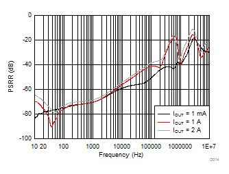
- PSRR: 70 dB at 1 kHz
- Power Good Output
- Create a Custom Design Using the LP5922 With the WEBENCH® Power Designer
2 Applications
- Space-Constrained Applications
- Noise- and Ripple-Sensitive High Current Analog or RF Systems
- Target Sectors
- Medical, Test and Measurement Equipment
- Portable and Consumer electronics
- Telecom and Networking Cards
- Wireless Infrastructure
- Industrial Applications
- Typical Systems
- Radio Transceivers, Power Amplifiers, PLL/Synthesizer, Clocking, VCO, GPRS, 3G Modules, FPGAs, DSP, GPUs, and others
3 Description
The LP5922 is 2-A low dropout (LDO) linear regulator with 200-mV typical dropout voltage at maximum current levels. The LP5922 device can operate from a voltage rail down to 1.3 V without additional bias supply. System efficiency is maximized and power dissipation minimized by the low dropout and low VIN capability. The device also features low quiescent current and very low shutdown current.
The LP5922 device was designed to have high PSRR and low output noise to support sensitive analog applications without additional filtering. The output noise can be reduced even further by implementing a small capacitor on the SS/NR pin.
The output voltage is adjustable from 0.5 V to 5 V by an external resistor divider. Enable pin, adjustable soft start and optional Power Good features help with system power sequencing. Inrush current is controlled with the soft start and the device has short circuit and thermal protections.
Device Information(1)
| PART NUMBER | PACKAGE | BODY SIZE (NOM) |
|---|---|---|
| LP5922 | WSON (10) | 3.00 mm × 3.00 mm |
- For all available packages, see the orderable addendum at the end of the data sheet.
space
space
space
space
space
space
space
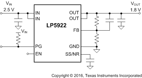
Simplified Schematic

PSRR
