SNOSD36A August 2017 – December 2017 LPV821
PRODUCTION DATA.
- 1 Features
- 2 Applications
- 3 Description
- 4 Revision History
- 5 Description (continued)
- 6 Pin Configuration and Functions
- 7 Specifications
- 8 Detailed Description
- 9 Application and Implementation
- 10Power Supply Recommendations
- 11Layout
- 12Device and Documentation Support
- 13Mechanical, Packaging, and Orderable Information
Package Options
Mechanical Data (Package|Pins)
- DBV|5
Thermal pad, mechanical data (Package|Pins)
Orderable Information
8.4.2 Driving Capacitive Load
The LPV821 is internally compensated for stable unity-gain operation, with a 8-kHz typical gain bandwidth. However, the unity-gain follower is the most sensitive configuration-to-capacitive load. The combination of a capacitive load placed directly on the output of an amplifier along with the output impedance of the amplifier creates a phase lag, which reduces the phase margin of the amplifier. If the phase margin is significantly reduced, the response is under-damped, which causes peaking in the transfer and, when there is too much peaking, the op amp might start oscillating.
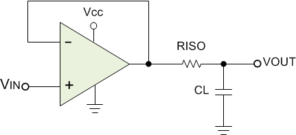
 Figure 38. Resistive Isolation of Capacitive Load
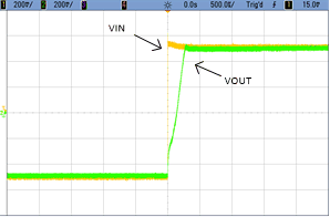
In order to drive heavy (> 50 pF) capacitive loads, use an isolation resistor, RISO, as shown in Figure 38. The value of the RISO to be used should be decided depending on the size of the CLand the level of performance desired. Recommended minimum values for RISO are given in the following table, for 3.3V supply. Figure 39 shows the typical response obtained with the CL = 50 pF RISO = 160 kΩ. By using the isolation resistor, the capacitive load is isolated from the output of the amplifier. The larger the value of RISO, the more stable the amplifier will be. If the value of RISO is sufficiently large, the feedback loop is stable, independent of the value of CL. However, larger values of RISO (e.g. 50 kΩ) result in reduced output swing and reduced output current drive.
Table 1. Capacitive Loads vs. Needed Isolation Resistors
| CL | RISO |
|---|---|
| 0 – 20 pF | not needed |
| 50 pF | 160 kΩ |
| 100 pF | 140 kΩ |
| 500 pF | 54.9 kΩ |
| 1 nF | 33 kΩ |
| 5 nF | 15 kΩ |
| 10 nF | 5.62 kΩ |
 Figure 39. Typical Step Response