SBAS803A November 2016 – November 2017 MUX506 , MUX507
PRODUCTION DATA.
- 1 Features
- 2 Applications
- 3 Description
- 4 Revision History
- 5 Pin Configuration and Functions
- 6 Specifications
- 7 Parameter Measurement Information
- 8 Detailed Description
- 9 Application and Implementation
- 10Power Supply Recommendations
- 11Layout
- 12Device and Documentation Support
- 13Mechanical, Packaging, and Orderable Information
Package Options
Mechanical Data (Package|Pins)
Thermal pad, mechanical data (Package|Pins)
Orderable Information
1 Features
- Low On-Capacitance
- MUX506: 13.5 pF
- MUX507: 8.7 pF
- Low Input Leakage: 1 pA
- Low Charge Injection: 0.31 pC
- Rail-to-Rail Operation
- Wide Supply Range: ±5 V to ±18 V, 10 V to 36 V
- Low On-Resistance: 125 Ω
- Transition Time: 97 ns
- Break-Before-Make Switching Action
- EN Pin Connectable to VDD
- Logic Levels: 2 V to VDD
- Low Supply Current: 45 µA
- ESD Protection HBM: 2000 V
- Industry-Standard TSSOP/ SOIC Package
2 Applications
- Factory Automation and Industrial Process Control
- Programmable Logic Controllers (PLC)
- Analog Input Modules
- ATE Test Equipment
- Digital Multimeters
- Battery Monitoring Systems
3 Description
The MUX506 and MUX507 (MUX50x) are modern complementary metal-oxide semiconductor (CMOS) precision analog multiplexers (muxes). The MUX506 offers 16:1 single-ended channels, whereas the MUX507 offers differential 8:1 or dual 8:1 single-ended channels. The MUX506 and MUX507 work equally well with either dual supplies (±5 V to ±18 V) or a single supply (10 V to 36 V). These devices also perform well with symmetric supplies (such as VDD = 12 V, VSS = –12 V), and unsymmetric supplies (such as VDD = 12 V, VSS = –5 V). All digital inputs have transistor-transistor logic (TTL) compatible thresholds, providing both TTL and CMOS logic compatibility when operating in the valid supply voltage range.
The MUX507 and MUX507 have very low on- and off-leakage currents, allowing these multiplexers to switch signals from high input impedance sources with minimal error. A low supply current of 45 µA enables use in power-sensitive applications.
Device Information(1)
| PART NUMBER | PACKAGE | BODY SIZE (NOM) |
|---|---|---|
| MUX506 MUX507 |
TSSOP (28) | 9.70 mm × 6.40 mm |
| SOIC (28) | 17.9 mm × 7.50 mm |
- For all available packages, see the package option addendum at the end of the data sheet.
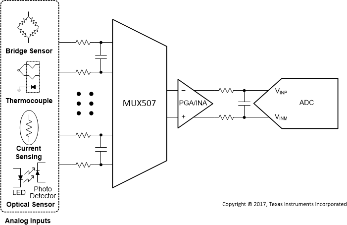
Simplified Schematic

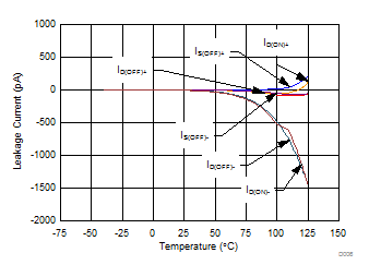
Leakage Current vs Temperature
