SLFS022I September 1973 – September 2014 NA555 , NE555 , SA555 , SE555
PRODUCTION DATA.
- 1 Features
- 2 Applications
- 3 Description
- 4 Simplified Schematic
- 5 Revision History
- 6 Pin Configuration and Functions
- 7 Specifications
- 8 Detailed Description
- 9 Applications and Implementation
- 10Power Supply Recommendations
- 11Device and Documentation Support
- 12Mechanical, Packaging, and Orderable Information
Package Options
Mechanical Data (Package|Pins)
Thermal pad, mechanical data (Package|Pins)
- PS|8
Orderable Information
9 Applications and Implementation
NOTE
Information in the following applications sections is not part of the TI component specification, and TI does not warrant its accuracy or completeness. TI’s customers are responsible for determining suitability of components for their purposes. Customers should validate and test their design implementation to confirm system functionality.
9.1 Application Information
The xx555 timer devices use resistor and capacitor charging delay to provide a programmable time delay or operating frequency. This section presents a simplified discussion of the design process.
9.2 Typical Applications
9.2.1 Missing-Pulse Detector
The circuit shown in Figure 16 can be used to detect a missing pulse or abnormally long spacing between consecutive pulses in a train of pulses. The timing interval of the monostable circuit is re-triggered continuously by the input pulse train as long as the pulse spacing is less than the timing interval. A longer pulse spacing, missing pulse, or terminated pulse train permits the timing interval to be completed, thereby generating an output pulse as shown in Figure 17.
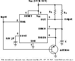 Figure 16. Circuit for Missing-Pulse Detector
9.2.1.1 Design Requirements
Input fault (missing pulses) must be input high. Input stuck low will not be detected because timing capacitor "C" will remain discharged.
9.2.1.2 Detailed Design Procedure
Choose RA and C so that RA× C > [maximum normal input high time]. RL improves VOH, but it is not required for TTL compatibility.
9.2.1.3 Application Curves
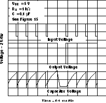 Figure 17. Completed Timing Waveforms for Missing-Pulse Detector
9.2.2 Pulse-Width Modulation
The operation of the timer can be modified by modulating the internal threshold and trigger voltages, which is accomplished by applying an external voltage (or current) to CONT. Figure 18 shows a circuit for pulse-width modulation. A continuous input pulse train triggers the monostable circuit, and a control signal modulates the threshold voltage. Figure 19 shows the resulting output pulse-width modulation. While a sine-wave modulation signal is shown, any wave shape could be used.
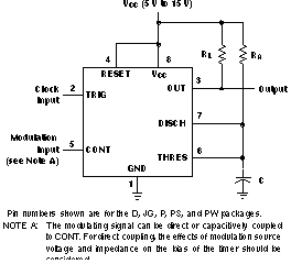 Figure 18. Circuit for Pulse-Width Modulation
9.2.2.1 Design Requirements
Clock input must have VOL and VOH levels that are less than and greater than 1/3 VCC. Modulation input can vary from ground to VCC. The application must be tolerant of a nonlinear transfer function; the relationship between modulation input and pulse width is not linear because the capacitor charge is based RC on an negative exponential curve.
9.2.2.2 Detailed Design Procedure
Choose RA and C so that RA × C = 1/4 [clock input period]. RL improves VOH, but it is not required for TTL compatibility.
9.2.2.3 Application Curves
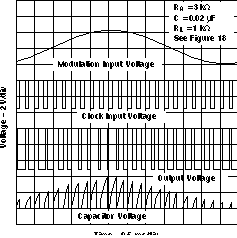 Figure 19. Pulse-Width-Modulation Waveforms
9.2.3 Pulse-Position Modulation
As shown in Figure 20, any of these timers can be used as a pulse-position modulator. This application modulates the threshold voltage and, thereby, the time delay, of a free-running oscillator. Figure 21 shows a triangular-wave modulation signal for such a circuit; however, any wave shape could be used.
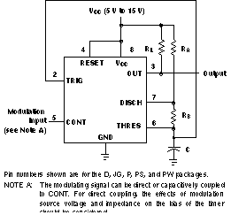 Figure 20. Circuit for Pulse-Position Modulation
9.2.3.1 Design Requirements
Both DC and AC coupled modulation input will change the upper and lower voltage thresholds for the timing capacitor. Both frequency and duty cycle will vary with the modulation voltage.
9.2.3.2 Detailed Design Procedure
The nominal output frequency and duty cycle can be determined using formulas in A-stable Operation section. RL improves VOH, but it is not required for TTL compatibility.
9.2.3.3 Application Curves
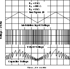 Figure 21. Pulse-Position-Modulation Waveforms
9.2.4 Sequential Timer
Many applications, such as computers, require signals for initializing conditions during start-up. Other applications, such as test equipment, require activation of test signals in sequence. These timing circuits can be connected to provide such sequential control. The timers can be used in various combinations of astable or monostable circuit connections, with or without modulation, for extremely flexible waveform control. Figure 22 shows a sequencer circuit with possible applications in many systems, and Figure 23 shows the output waveforms.
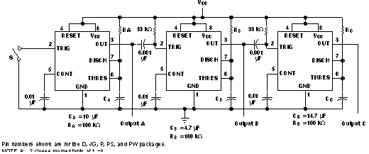 Figure 22. Sequential Timer Circuit
9.2.4.1 Design Requirements
The sequential timer application chains together multiple mono-stable timers. The joining components are the 33-kΩ resistors and 0.001-µF capacitors. The output high to low edge passes a 10-µs start pulse to the next monostable.
9.2.4.2 Detailed Design Procedure
The timing resistors and capacitors can be chosen using this formula. tw = 1.1 × R × C.
9.2.4.3 Application Curves
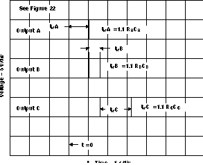 Figure 23. Sequential Timer Waveforms