SBAS796 July 2017 ONET2804TLP
PRODUCTION DATA.
- 1 Features
- 2 Applications
- 3 Description
- 4 Revision History
- 5 Pin Configuration and Functions
- 6 Specifications
-
7 Detailed Description
- 7.1 Overview
- 7.2 Functional Block Diagram
- 7.3 Feature Description
- 7.4 Device Functional Modes
- 7.5 Programming
- 7.6
Register Maps
- 7.6.1 Register Descriptions
- 7.6.2 Register 0: Control Settings (address = 00h) [reset = 0h]
- 7.6.3 Register 1: Amplitude and Rate for Channel 1 (address = 01h) [reset = 0h]
- 7.6.4 Register 2: Threshold and Gain for Channel 1 (address = 02h) [reset = 0h]
- 7.6.5 Register 7: Amplitude and Rate for Channel 2 (address = 07h) [reset = 0h]
- 7.6.6 Register 8: Threshold and Gain for Channel 1 (address = 08h) [reset = 0h]
- 7.6.7 Register 13: Amplitude and Rate for Channel 3 (address = 0Dh) [reset = 0h]
- 7.6.8 Register 14: Threshold and Gain for Channel 3 (address = 0Eh) [reset = 0h]
- 7.6.9 Register 19: Amplitude and Rate for Channel 4 (address = 13h) [reset = 0h]
- 7.6.10 Register 20: Threshold and Gain for Channel 4 (address = 14h) [reset = 0h]
- 8 Application and Implementation
- 9 Power Supply Recommendations
- 10Layout
- 11Device and Documentation Support
- 12Mechanical, Packaging, and Orderable Information
Package Options
Mechanical Data (Package|Pins)
- Y|0
Thermal pad, mechanical data (Package|Pins)
Orderable Information
6 Specifications
6.1 Absolute Maximum Ratings
over operating free-air temperature range (unless otherwise noted)(1)| MIN | MAX | UNIT | ||
|---|---|---|---|---|
| Supply voltage(1) | VCCIx, VCCOx | –0.3 | 4 | V |
| Voltage(1) | FILTERx, OUTx+, OUTx–, RSSIx, SCL, SDA, I2CENA, ICC_ADJ, AMPL, RATE, GAIN, TRSH, ADR1, ADR0, and NRESET | –0.3 | 4 | V |
| Average input current | INx | –0.7 | 5 | mA |
| FILTERx | –8 | 8 | mA | |
| Continuous current at outputs | OUTx+, OUTx– | –8 | 8 | mA |
| Maximum junction temperature, TJ | 125 | °C | ||
| Storage temperature, Tstg | –65 | 150 | °C | |
(1) All voltage values are with respect to network ground terminal.
6.2 ESD Ratings
| VALUE | UNIT | ||||
|---|---|---|---|---|---|
| V(ESD) | Electrostatic discharge | Human-body model (HBM), per ANSI/ESDA/JEDEC JS-001(1) | All pins except INx | ±1000 | V |
| INx pins | ±500 | ||||
(1) JEDEC document JEP155 states that 500-V HBM allows safe manufacturing with a standard ESD control process.
6.3 Recommended Operating Conditions
over operating free-air temperature range (unless otherwise noted)| MIN | NOM | MAX | UNIT | |||
|---|---|---|---|---|---|---|
| VCC | Supply voltage | 2.8 | 3.3 | 3.47 | V | |
| I(INx) | Average input current | 2.7 | mA | |||
| TA | Operating backside die temperature | –40 | 100 | °C | ||
| L(FILTER), L(IN) | Wire-bond inductance at the FILTERx and INx pins | 0.3 | nH | |||
| C(PD) | Photodiode capacitance | 0.1 | pF | |||
| VIH | Digital input high voltage | SDA, SCL | 2 | V | ||
| VIL | Digital input low voltage | SDA, SCL | 0.8 | V | ||
| 3-state input high voltage | VCC – 0.4 | V | ||||
| 3-state input low voltage | 0.4 | V | ||||
6.4 DC Electrical Characteristics
over recommended operating conditions with VOD = 300 mVPP (unless otherwise noted); typical values are at VCC = 3.3 V and TA = 25°C| PARAMETER | TEST CONDITIONS | MIN | TYP | MAX | UNIT | TEST LEVEL(3) | |
|---|---|---|---|---|---|---|---|
| VCC | Supply voltage | 2.8 | 3.3 | 3.47 | V | A | |
| ICC | Supply current | Per channel, 30-μAPP input, 27°C | 22 | 42 | mA | A | |
| Per channel, 30-μAPP input, maximum 85°C | 30 | C | |||||
| Per channel, 30-μAPP input, maximum 100°C | 36 | C | |||||
| P(RX) | Receiver power dissipation | Per channel, 30-μAPP input, 27°C | 73 | 139 | mW | A | |
| Per channel, 30-μAPP input, maximum 85°C | 99 | C | |||||
| Per channel, 30-μAPP input, maximum 100°C | 118 | C | |||||
| VIN | Input bias voltage | 0.75 | 0.85 | 0.98 | V | A | |
| ROUT | Output resistance | Single-ended to VCC | 40 | 50 | 60 | Ω | A |
| V(FILTER) | Photodiode bias voltage(1) | 2.8 | 3.2 | V | A | ||
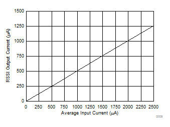
| A(RSSI_IB) | RSSI gain | Resistive load to GND(2) | 0.49 | 0.5 | 0.54 | A/A | A |
| RSSIx feature output offset current (no light) | 0 | 2.5 | µA | A | |||
(1) Regulated voltage is typically 100 mV lower than VCC.
(2) The RSSIx output is a current output that requires a resistive load to ground (GND). The voltage gain can be adjusted for the intended application by choosing the external resistor; however, for proper operation, ensure that the voltage at RSSIx does not exceed VCC – 0.65 V.
(3) Test levels: (A) 100% tested at 25°C. Overtemperature limits set by characterization and simulation. (B) Limits set by characterization and simulation. (C) Typical value only for information.
6.5 AC Electrical Characteristics
over recommended operating conditions with VOD = 300 mVPP (unless otherwise noted); typical values are at VCC = 3.3 V and TA = 25°C| PARAMETER | TEST CONDITIONS | MIN | TYP | MAX | UNIT | TEST LEVEL(5) | |
|---|---|---|---|---|---|---|---|
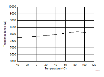
| Z21 | Small-signal transimpedance | 25-μAPP input signal | 7.5 | kΩ | C | ||
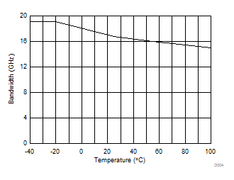
| f(3dB-H) | –3-dB bandwidth | 25-μAPP input signal(1) | 17.5 | GHz | C | ||
| f(3dB-L) | Low-frequency, –3-dB bandwidth | 30 | kHz | C | |||
| iN(IN) | Input-referred RMS noise | CPD = 0.1 pF, 28-GHz BT4 filter(2) | 2 | μA | C | ||
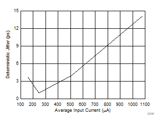
| DJ | Deterministic jitter | 35 µAPP < iIN < 250 µAPP
(27.95 Gbps, PRBS9 pattern) |
2 | psPP | C | ||
| 250 µAPP < iIN < 500 µAPP
(27.95 Gbps, PRBS9 pattern) |
2 | C | |||||
| 500 µAPP < iIN < 2900 µAPP
(27.95 Gbps, PRBS9 pattern) |
4 | C | |||||
| VOD | Differential output voltage | 500-mVPP setting | 250 | 500 | 700 | mVPP | C |
| Crosstalk | Between adjacent channels, up to 20 GHz(3) | –40 | dB | C | |||
| RSSIx response time | 1 | μs | C | ||||
| PSRR | Power-supply rejection ratio | f < 10 MHz(4) | –15 | dB | C | ||
(1) The small-signal bandwidth is specified over process corners, temperature, and supply voltage variation. The assumed photodiode capacitance is 0.1 pF and the bond-wire inductance is 0.3 nH. The small-signal bandwidth strongly depends on environmental parasitics. Careful attention to layout parasitics and external components is necessary to achieve optimal performance.
(2) Input-referred RMS noise is (RMS output noise) / (gain at 100 MHz).
(3) Die only, no wire bonds.
(4) PSRR is the differential output amplitude divided by the voltage ripple on the supply. No input current at INx.
(5) Test levels: (A) 100% tested at 25°C. Overtemperature limits set by characterization and simulation. (B) Limits set by characterization and simulation. (C) Typical value only for information.
6.6 Timing Requirements
| MIN | NOM | MAX | UNIT | ||
|---|---|---|---|---|---|
| fSCK | SCK clock frequency | 400 | kHz | ||
| tBUF | Bus free time between START and STOP conditions | 1.3 | µs | ||
| tHDSTA | Hold time after repeated START condition. After this period, the first clock pulse is generated. | 0.6 | µs | ||
| tLOW | Low period of the SCK clock | 1.3 | µs | ||
| tHIGH | High period of the SCK clock | 0.6 | µs | ||
| tSUSTA | Setup time for a repeated START condition | 0.6 | µs | ||
| tHDDAT | Data hold time | 0 | µs | ||
| tSUDAT | Data setup time | 100 | ns | ||
| tR | Rise time of both SDA and SCK signals | 300 | ns | ||
| tF | Fall time of both SDA and SCK signals | 300 | ns | ||
| tSUSTO | Setup time for STOP condition | 0.6 | µs | ||
6.7 Typical Characteristics: General
typical operating condition is at VCC = 3.3 V, TA = 25°C, and VOD = 300 mVPP (unless otherwise noted)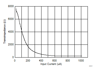
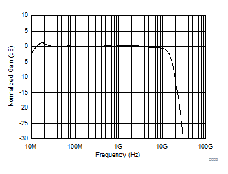
(Test Fixture Loss De-Embedded)
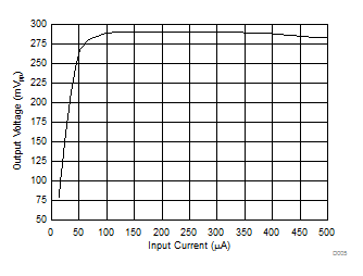
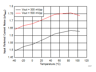
(Test Fixture Loss De-Embedded)
6.8 Typical Characteristics: Eye Diagrams
typical operating condition is at VCC = 3.3 V, TA = 25°C, and VOD = 500 mVPP (unless otherwise noted)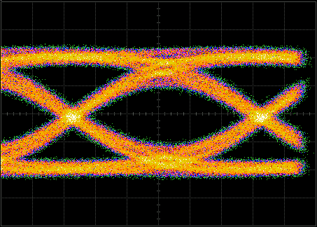
| 27.95 Gbps |
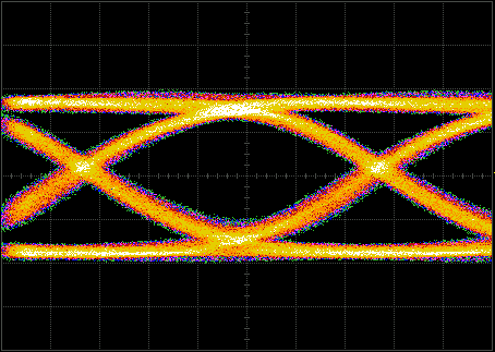
| 27.95 Gbps |
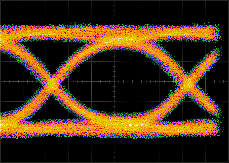
| 27.95 Gbps |
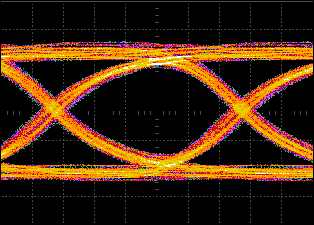
| 27.95 Gbps |