SBOS791A June 2017 – November 2017 OPA1641-Q1 , OPA1642-Q1
PRODUCTION DATA.
- 1 Features
- 2 Applications
- 3 Description
- 4 Revision History
- 5 Pin Configuration and Functions
- 6 Specifications
- 7 Detailed Description
- 8 Application and Implementation
- 9 Power Supply Recommendations
- 10Layout
- 11Device and Documentation Support
- 12Mechanical, Packaging, and Orderable Information
Package Options
Mechanical Data (Package|Pins)
- DGK|8
Thermal pad, mechanical data (Package|Pins)
- DGK|8
Orderable Information
8 Application and Implementation
NOTE
Information in the following applications sections is not part of the TI component specification, and TI does not warrant its accuracy or completeness. TI’s customers are responsible for determining suitability of components for their purposes. Customers should validate and test their design implementation to confirm system functionality.
8.1 Application Information
The OPA164x-Q1 amplifiers are unity-gain stable, audio operational amplifiers with very low noise, input bias current, and input offset voltage. Applications with noisy or high-impedance power supplies require decoupling capacitors placed close to the device pins. In most cases, 0.1-μF capacitors are adequate. Figure 32 shows a simplified schematic of the OPA1641-Q1.
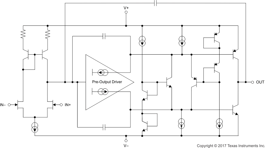 Figure 32. Simplified Internal Schematic
8.1.1 Total Harmonic Distortion Measurements
The OPA164x-Q1 series operational amplifiers have excellent distortion characteristics. THD + noise is below 0.00005% (G = 1, VO = 3 VRMS, BW = 80 kHz) throughout the audio frequency range, 20 Hz to 20 kHz, with a
2-kΩ load (see Figure 7).
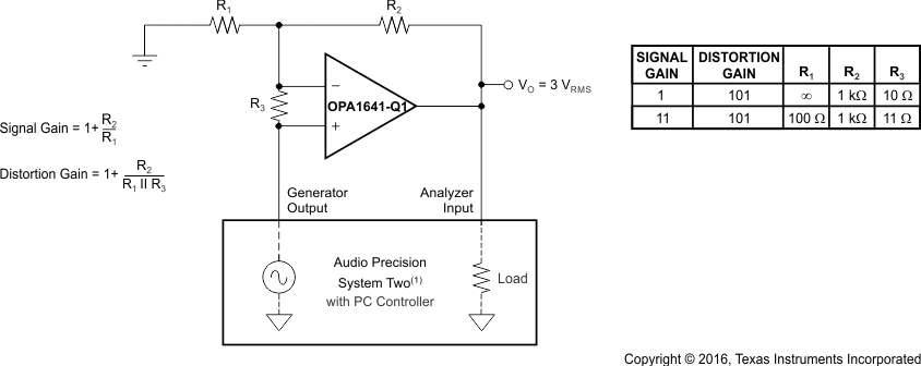
The distortion produced by the OPA164x-Q1 series op amps is below the measurement limit of many commercially available distortion analyzers. However, a special test circuit (such as shown in Figure 33) can be used to extend the measurement capabilities.
Operational amplifier distortion can be considered an internal error source that can be referred to the input. Figure 33 shows a circuit that causes the operational amplifier distortion to be 101 times (or approximately 40 dB) greater than that normally produced by the op amp. The addition of R3 to the otherwise standard noninverting amplifier configuration alters the feedback factor or noise gain of the circuit. The closed-loop gain is unchanged, but the feedback available for error correction is reduced by a factor of 101, extending the resolution by 101. The input signal and load applied to the op amp are the same as with conventional feedback without R3. Keep the value of R3 small to minimize any effect on distortion measurements.
The validity of this technique can be verified by duplicating measurements at high gain or high frequency where the distortion is within the measurement capability of the test equipment. Measurements for this document were made with an audio precision system two distortion and noise analyzer that greatly simplifies repetitive measurements. However, the measurement technique can be performed with manual distortion measurement instruments.
space
8.1.2 Source Impedance and Distortion
In traditional JFET-input op amps, the impedance applied to the positive and negative inputs in noninverting applications must be matched for lowest distortion. Legacy methods for fabricating the JFETs in the FET input stage exhibit a varying input capacitance with applied common-mode input voltage. In inverting configurations, the input does not vary with input voltage because the inverting input is held at virtual ground. However, in noninverting applications, the inputs do vary, and the gate-to-source voltage is not constant. This effect produces increased distortion resulting from the varying capacitance for unmatched source impedances. However, the OPA164x-Q1 family of amplifiers is designed to maintain a constant input capacitance with varying common-mode voltage to prevent this mechanism of distortion. The variation of input capacitance with common-mode voltage for a traditional amplifier is compared to the OPA164x-Q1 family in Figure 34.
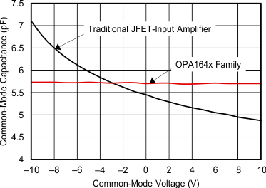 Figure 34. Input Capacitance of the OPA164x-Q1 Family of Amplifiers Compared to Traditional JFET-input Amplifiers
By stabilizing the input capacitance, the distortion performance of the amplifier is greatly improved for noninverting configurations with high source impedances. The measured performance of an OPA164x-Q1 amplifier is compared to a traditional JFET-input amplifier in Figure 35. The unity-gain configuration, high source impedance, and large-signal amplitude produce additional distortion in the traditional amplifier.
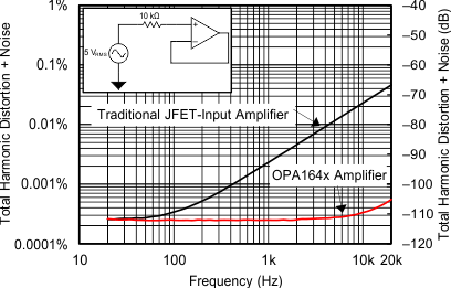 Figure 35. Measured THD+N of the OPA164x-Q1 Family of Amplifiers Compared to Traditional JFET-input Amplifiers
8.1.3 Capacitive Load and Stability
The dynamic characteristics of the OPA164x-Q1 are optimized for commonly encountered gains, loads, and operating conditions. The combination of low closed-loop gain and high capacitive loads decreases the phase margin of the amplifier and can lead to gain peaking or oscillations. As a result, heavier capacitive loads must be isolated from the output. The simplest way to achieve this isolation is to add a small resistor (ROUT equal to 50 Ω, for example) in series with the output.
Figure 19 and Figure 20 illustrate graphs of Small-Signal Overshoot vs Capacitive Load for several values of ROUT. For details of analysis techniques and application circuits, see see Feedback Plots Define Op Amp AC Performance available for download at www.ti.com
8.1.4 Power Dissipation and Thermal Protection
The OPA164x-Q1 op amps are capable of driving 2-kΩ loads with power-supply voltages of up to ±18 V over the specified temperature range. In a single-supply configuration, where the load is connected to the negative supply voltage, the minimum load resistance is 2.8 kΩ at a supply voltage of 36 V. For lower supply voltages (either single-supply or symmetrical supplies), a lower load resistance can be used, as long as the output current does not exceed 13 mA; otherwise, the device short-circuit current-protection circuit can activate.
Internal power dissipation increases when operating at high supply voltages. Copper leadframe construction used in the OPA164x-Q1 series of devices improves heat dissipation compared to conventional materials. PCB layout can help reduce a possible increase in junction temperature. Wide copper traces help dissipate the heat by functioning as an additional heat sink. Temperature rise can be further minimized by soldering the devices directly to the PCB rather than using a socket.
Although the output current is limited by internal protection circuitry, accidental shorting one or more output channels of a device can result in excessive heating. For instance, when an output is shorted to midsupply, the typical short-circuit current of 36 mA leads to an internal power dissipation of over 600 mW at a supply of ±18 V. In case of a dual OPA1642-Q1 in an VSSOP-8 package (thermal resistance RθJA = 180°C/W), such a power dissipation results in the die temperature to be 220°C above ambient temperature, when both channels are shorted. This temperature increase destroys the device.
To prevent such excessive heating that can destroy the device, the OPA164x-Q1 series has an internal thermal shutdown circuit that shuts down the device if the die temperature exceeds approximately 180°C. When this thermal shutdown circuit activates, a built-in hysteresis of 15°C ensures that the die temperature must drop to approximately 165°C before the device switches on again.
8.1.5 Electrical Overstress
Designers often ask questions about the capability of an operational amplifier to withstand electrical overstress. These questions tend to focus on the device inputs, but can involve the supply voltage pins or even the output pin. Each of these different pin functions have electrical stress limits determined by the voltage breakdown characteristics of the particular semiconductor fabrication process and specific circuits connected to the pin. Additionally, internal electrostatic discharge (ESD) protection is built into these circuits to protect them from accidental ESD events both before and during product assembly.
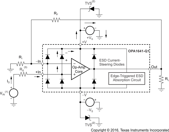
Having a good understanding of this basic ESD circuitry and the relevance to an electrical overstress event is helpful. Figure 36 illustrates the ESD circuits contained in the OPA164x-Q1 series (indicated by the dashed line area). The ESD protection circuitry involves several current-steering diodes connected from the input and output pins and routed back to the internal power-supply lines where an internal absorption device is connected. This protection circuitry is intended to remain inactive during normal circuit operation.
An ESD event produces a short-duration, high-voltage pulse that is transformed into a short-duration, high-current pulse when discharging through a semiconductor device. The ESD protection circuits are designed to provide a current path around the operational amplifier core to prevent damage. The energy absorbed by the protection circuitry is then dissipated as heat.
When an ESD voltage develops across two or more of the amplifier device pins, current flows through one or more of the steering diodes. Depending on the path that the current takes, the absorption device can activate. The absorption device has a trigger (or threshold voltage) that is above the normal operating voltage of the OPA164x-Q1 but below the device breakdown voltage level. When this threshold is exceeded, the absorption device quickly activates and clamps the voltage across the supply rails to a safe level.
When the operational amplifier connects into a circuit as shown in Figure 36, the ESD protection components are intended to remain inactive and not become involved in the application circuit operation. However, circumstances can arise where an applied voltage exceeds the operating voltage range of a given pin. If this condition occurs, some of the internal ESD protection circuits can be biased on and conduct current. Any such current flow occurs through steering diode paths and rarely involves the absorption device.
Figure 36 depicts a specific example where the input voltage (VIN) exceeds the positive supply voltage (+VS) by 500 mV or more. Much of what happens in the circuit depends on the supply characteristics. If +VS can sink the current, one of the upper input steering diodes conducts and directs current to +VS. Excessively high current levels can flow with increasingly higher VIN. As a result, the data sheet specifications recommend that applications limit the input current to 10 mA.
If the supply is not capable of sinking the current, VIN can begin sourcing current to the operational amplifier, and then take over as the source of positive supply voltage. The danger in this case is that the voltage can rise to levels that exceed the operational amplifier absolute maximum ratings.
Another common question involves what happens to the amplifier if an input signal is applied to the input when the power supplies +VS and –VS are at 0 V. The amplifier behavior depends on the supply characteristic when at 0 V, or at a level below the input signal amplitude. If the supplies appear as high impedance, then the operational amplifier supply current can be supplied by the input source through the current steering diodes. This state is not a normal bias condition; the amplifier most likely does not operate normally. If the supplies are low impedance, then the current through the steering diodes can become quite high. The current level depends on the ability of the input source to deliver current and any resistance in the input path.
If there is an uncertainty about the ability of the supply to absorb this current, external Zener diodes can be added to the supply pins, as shown in Figure 36. The Zener voltage must be selected so the diode does not turn on during normal operation. However, the Zener voltage must be low enough so that the Zener diode conducts if the supply pin begins to rise above the safe operating supply voltage level.
8.2 Typical Application
8.2.1 Single-Supply Electret Microphone Preamplifier for Speech
Electret microphones are commonly used in automotive hands-free phone systems because of their small size, low cost, and relatively good signal-to-noise ratio (SNR). The low noise and distortion of the OPA1641-Q1 makes the device a good choice for preamplifier circuits for electret microphones. The circuit shown in Figure 37 is a single-supply preamplifier circuit for electret microphones with a bandwidth from 100 Hz to 3 kHz for capturing speech.
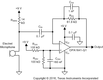 Figure 37. Preamplifier Circuit for Electret Microphones Using a Single Power Supply Voltage
8.2.1.1 Design Requirements
- 9-V single supply
- 1-VRMS output for 100-dBSPL input
- Approximately 100-Hz to 3-kHz, –3-dB Bandwidth
- Microphone sensitivity: 8 µA / Pa
- Microphone operating voltage: 2 V to 10 V
- Microphone bias current: 500 µA
8.2.1.2 Detailed Design Procedure
In this circuit, the op amp is configured as a transimpedance amplifier which converts the signal current of the microphone into an output voltage. The bandwidth of this circuit is limited to the vocal range as is common in telephony systems. The gain of the circuit is determined by the feedback resistor (RFB), which must be calculated according to the microphone sensitivity. For this design, a microphone output current of 8 µA per Pascal (Pa) of air pressure was selected. Using this value, the output current for a sound pressure level of 100 dBSPL, or 2 Pa air pressure, is calculated in Equation 1.

RFB is then calculated from this current to produce 1-VRMS output for a 100-dBSPL input signal in Equation 2.

The feedback capacitor (CFB) is calculated to limit the bandwidth of the amplifier to 3 kHz in Equation 3.

RBIAS is necessary to divert the microphone signal current through capacitor CIN rather than flowing from the power supply (VCC). Larger values of RBIAS allow for a smaller capacitor to be used for CIN and reduces the overall noise of the circuit. However, the maximum value for RBIAS is limited by the microphone bias current and minimum operating voltage.
The value of RBIAS is calculated in Equation 4.

Input capacitor CIN forms a high-pass filter in combination with resistor RBIAS. The filter corner frequency calculation is shown in Equation 5 to place the high-pass corner frequency at 100 Hz.

The voltage divider network at the op amp noninverting input is used to bias the op amp output to the midsupply point (VCC / 2) to maximize the output voltage range of the circuit. This result is easily achieved by selecting the same value for both resistors in the divider. The absolute value of those resistors is limited by the acceptable power-supply current drawn by the voltage divider. Choosing 50 µA as an acceptable limit of supply current gives a value of 100 kΩ for the resistors in the divider, as Equation 6 shows.

Finally, to minimize the additional noise contribution from the voltage divider, a capacitor is placed at the op amp noninverting input. This capacitor forms a low-pass filter with the parallel combination of the voltage divider resistors. Selecting a filter corner frequency of 20 Hz minimizes the noise contribution of the voltage divider inside the amplifier passband; see Equation 7.

8.2.1.3 Application Curve
The transfer function of the microphone preamplifier circuit is shown in Figure 38. The nominal gain of the circuit is 95.46 dB, or 59,292.5 V per amp of input current. The –3-dB bandwidth limits of the circuit are 105.7 Hz and 2.77 kHz.
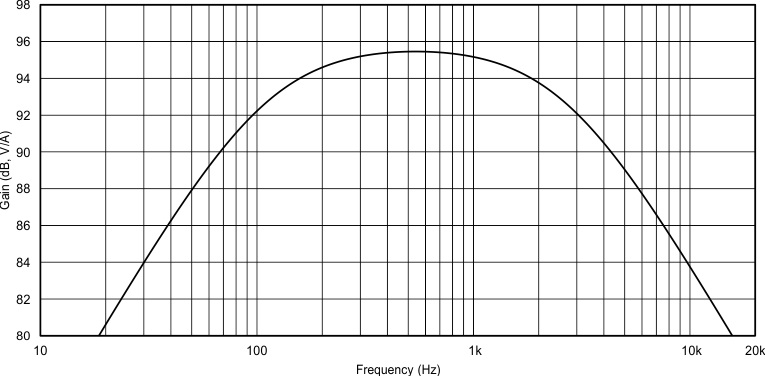 Figure 38. Microphone Preamplifier Transfer Function
