SBOS054B January 1995 – September 2015 OPA132 , OPA2132 , OPA4132
PRODUCTION DATA.
- 1 Features
- 2 Applications
- 3 Description
- 4 Revision History
- 5 Pin Configuration and Functions
- 6 Specifications
- 7 Detailed Description
- 8 Application and Implementation
- 9 Power Supply Recommendations
- 10Layout
- 11Device and Documentation Support
- 12Mechanical, Packaging, and Orderable Information
Package Options
Mechanical Data (Package|Pins)
Thermal pad, mechanical data (Package|Pins)
- D|8
Orderable Information
8 Application and Implementation
NOTE
Information in the following applications sections is not part of the TI component specification, and TI does not warrant its accuracy or completeness. TI’s customers are responsible for determining suitability of components for their purposes. Customers should validate and test their design implementation to confirm system functionality.
8.1 Application Information
The OPAx132 series operational amplifiers are unity-gain stable and suitable for a wide range of general-purpose applications. Power supply pins should be bypassed with 10-nF ceramic capacitors or larger.
The OPAx132 series operational amplifiers are free from unexpected output phase reversal common with FET operational amplifiers. Many FET-input operational amplifiers exhibit phase-reversal of the output when the input common-mode voltage range is exceeded. This can occur in voltage-follower circuits, causing serious problems in control loop applications. The OPAx132 series of operational amplifiers are free from this undesirable behavior. All circuitry is completely independent in dual and quad versions, assuring normal behavior when one amplifier in a package is overdriven or short-circuited.
8.1.1 Operating Voltage
The OPAx132 series of operation amplifiers operate with power supplies from ±2.5 V to ±18 V with excellent performance. Although specifications are production tested with ±15 V supplies, most behavior remains unchanged throughout the full operating voltage range. Parameters which vary significantly with operating voltage are shown in the Typical Characteristics section.
8.1.2 Offset Voltage Trim
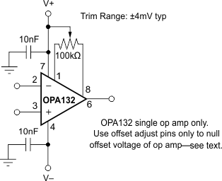
Offset voltage of the OPAx132 series of amplifiers is laser trimmed and usually requires no user adjustment. The OPAx132 amplifier (single op amp version) provides offset voltage trim connections on pins 1 and 8. Offset voltage can be adjusted by connecting a potentiometer as shown in Figure 18. This adjustment should be used only to null the offset of the operational amplifier, not to adjust system offset or offset produced by the signal source. Nulling offset could degrade the offset voltage drift behavior of the operational amplifier. While it is not possible to predict the exact change in drift, the effect is usually small.
 Figure 18. OPAx132 Offset Voltage Trim Circuit
8.1.3 Input Bias Current
The FET-inputs of the OPAx132 series provide very low input bias current and cause negligible errors in most applications. For applications where low input bias current is crucial, junction temperature rise should be minimized. The input bias current of FET-input operational amplifiers increases with temperature as shown in Figure 5.
The OPAx132 series may be operated at reduced power supply voltage to minimize power dissipation and temperature rise. Using ±3 V supplies reduces power dissipation to one-fifth that at ±15 V.
The dual and quad versions have higher total power dissipation than the single, leading to higher junction temperature. Thus, a warmed-up quad will have higher input bias current than a warmed-up single. Furthermore, an SOIC will generally have higher junction temperature than a DIP at the same ambient temperature because of a larger θJA.
Printed-circuit-board layout can also help minimize junction temperature rise. Temperature rise can be minimized by soldering the devices to the circuit board rather than using a socket. Wide copper traces will also help dissipate the heat by acting as an additional heat sink.
Input stage cascode circuitry assures that the input bias current remains virtually unchanged throughout the full input common-mode range of the OPAx132 series. See Figure 6.
8.2 Typical Application
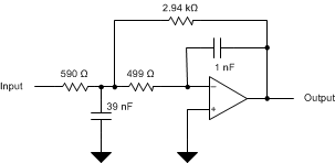
The OPAx132 family offers outstanding dc precision and ac performance. These devices operate up to 36-V supply rails and offer ultralow input bias current and input bias current noise, as well as 8-MHz bandwidth and high capacitive load drive. These features make the OPAx132 a robust, high-performance operational amplifier for high-voltage industrial applications with high source impedance.
 Figure 19. OPA132 2nd Order 30 kHz, Low Pass Filter Schematic
8.2.1 Design Requirements
Use the following parameters for this application:
- Gain = 5 V/V
- Low pass cutoff frequency = 30 kHz
- -40 db/dec filter response
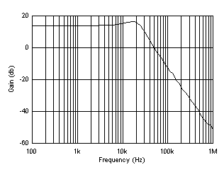
- Maintain less than 3-dB gain peaking in the gain versus frequency response
8.2.2 Detailed Design Procedure
WEBENCH® Filter Designer is a simple, powerful, and easy-to-use active filter design program. The WEBENCH Filter Designer lets you create optimized filter designs using a selection of TI operational amplifiers and passive components from TI's vendor partners.
Available as a web based tool from the WEBENCH® Design Center, WEBENCH® Filter Designer allows you to design, optimize, and simulate complete multistage active filter solutions within minutes.
8.2.3 Application Curve
 Figure 20. OPA132 2nd Order 30-kHz, Low Pass Filter Response