SBOS860 April 2017 OPA188-Q1 , OPA2188-Q1
PRODUCTION DATA.
- 1 Features
- 2 Applications
- 3 Description
- 4 Revision History
- 5 Device Comparison Table
- 6 Pin Configuration and Functions
- 7 Specifications
- 8 Detailed Description
- 9 Application and Implementation
- 10Power Supply Recommendations
- 11Layout
- 12Device and Documentation Support
- 13Mechanical, Packaging, and Orderable Information
Package Options
Mechanical Data (Package|Pins)
- DGK|8
Thermal pad, mechanical data (Package|Pins)
- DGK|8
Orderable Information
9 Application and Implementation
NOTE
Information in the following applications sections is not part of the TI component specification, and TI does not warrant its accuracy or completeness. TI’s customers are responsible for determining suitability of components for their purposes. Customers should validate and test their design implementation to confirm system functionality.
9.1 Application Information
The OPAx188-Q1 operational amplifiers combine precision offset and drift with excellent overall performance, making the series ideal for many precision applications. The precision offset drift of only 0.085 µV/°C provides stability over the entire temperature range. In addition, the device pairs excellent CMRR, PSRR, and AOL dc performance with outstanding low-noise operation. As with all amplifiers, applications with noisy or high-impedance power supplies require decoupling capacitors close to the device pins. In most cases, 0.1-µF capacitors are adequate.
The following application examples highlight only a few of the circuits where the OPAx188-Q1 series can be used.
9.2 Typical Applications
9.2.1 High-Side Voltage-to-Current (V-I) Converter
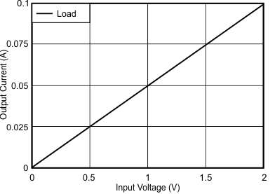
The circuit shown in Figure 43 is a high-side voltage-to-current (V-I) converter. The converter translates an input voltage of 0 V to 2 V to an output current of 0 mA to 100 mA. Figure 44 shows the measured transfer function for this circuit. The low offset voltage and offset drift of the OPA2188-Q1 facilitate excellent dc accuracy for the circuit.
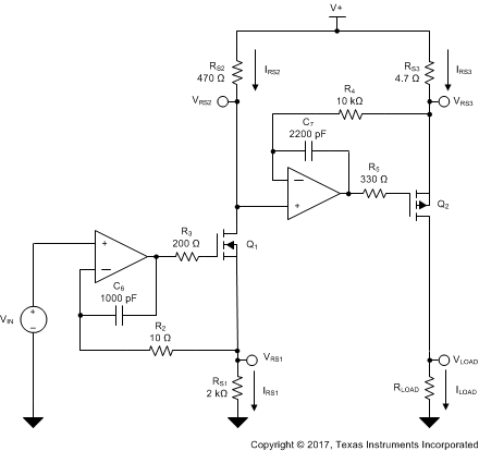 Figure 43. High-Side Voltage-to-Current (V-I) Converter
9.2.1.1 Design Requirements
The design requirements are:
- Supply voltage: 5 V dc
- Input: 0 V to 2 V dc
- Output: 0 mA to 100 mA dc
9.2.1.2 Detailed Design Procedure
The V-I transfer function of the circuit is based on the relationship between the input voltage, VIN, and the three current sensing resistors, RS1, RS2, and RS3. The relationship between VIN and RS1 determines the current that flows through the first stage of the design. The current gain from the first stage to the second stage is based on the relationship between RS2 and RS3.
For a successful design, pay close attention to the dc characteristics of the operational amplifier chosen for the application. To meet the performance goals, this application benefits from an operational amplifier with low offset voltage, low temperature drift, and rail-to-rail output. The OPAx188-Q1 CMOS operational amplifier is a high-precision, ultra-low offset, ultra-low drift amplifier, optimized for low-voltage, single-supply operation, with an output swing to within 15 mV of the positive rail. The devices in the OPAx188-Q1 family use chopping techniques to provide low initial offset voltage and near-zero drift over time and temperature. Low offset voltage and low drift reduce the offset error in the system, making this device appropriate for precise dc control. The rail-to-rail output stage of the OPAx188-Q1 makes sure that the output swing of the operational amplifier is able to fully control the gate of the MOSFET devices within the supply rails.
A detailed error analysis, design procedure, and additional measured results are given in reference design TIPD102, a step-by-step process to design a High-Side Voltage-to-Current (V-I) Converter.
 |
For step-by-step design procedure, circuit schematics, bill of materials, PCB files, simulation results, and test results, refer to TI Precision Design TIPD102, High-Side Voltage-to-Current (V-I) Converter (SLAU502). |
9.2.2 Discrete INA + Attenuation for ADC With 3.3-V Supply
NOTE
The TINA-TI files shown in the following sections require that either the TINA software (from DesignSoft™) or TINA-TI software be installed. Download the free TINA-TI software from the TINA-TI folder.
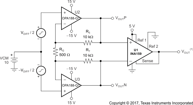
Figure 45 shows an example of how the OPA188-Q1 series is used as a high-voltage, high-impedance front-end for a precision, discrete instrumentation amplifier with attenuation. The INA159 provides the attenuation that allows this circuit to easily interface with 3.3-V or 5-V analog-to-digital converters (ADCs). Click the following link to download the TINA-TI file: Discrete INA.
9.2.3 Bridge Amplifier
Figure 46 shows the basic configuration for a bridge amplifier. Click the following link to download the TINA-TI file: Bridge Amplifier Circuit.
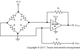 Figure 46. Bridge Amplifier
9.2.4 Low-Side Current Monitor
Figure 47 shows the OPAx188-Q1 configured in a low-side current-sensing application. The load current (ILOAD) creates a voltage drop across the shunt resistor (RSHUNT). This voltage is amplified by the OPAx188-Q1, with a gain of 201. The load current is set from 0 A to 500 mA, which corresponds to an output voltage range from 0 V to 10 V. The output range can be adjusted by changing the shunt resistor or gain of the configuration. Click the following link to download the TINA-TI file: Current-Sensing Circuit.
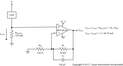 Figure 47. Low-Side Current Monitor
9.2.5 Programmable Power Supply
Figure 48 shows the OPA188-Q1 configured as a precision programmable power supply using the 16-bit, voltage output DAC8581 and the OPA548 high-current amplifier. This application amplifies the digital-to-analog converter (DAC) voltage by a value of five, and handles a large variety of capacitive and current loads. The OPA188-Q1 in the front-end provides precision and low drift across a wide range of inputs and conditions. Click the following link to download the TINA-TI file: Programmable Power-Supply Circuit.
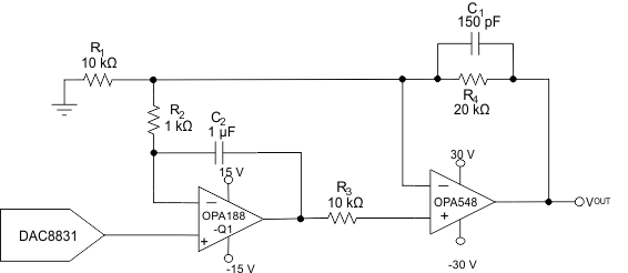 Figure 48. Programmable Power Supply
9.2.6 RTD Amplifier With Linearization
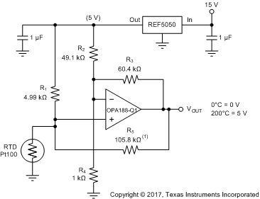
See Analog Linearization Of Resistance Temperature Detectors for an in-depth analysis of Figure 49. Click the following link to download the TINA-TI file: RTD Amplifier with Linearization.
