SBOS860 April 2017 OPA188-Q1 , OPA2188-Q1
PRODUCTION DATA.
- 1 Features
- 2 Applications
- 3 Description
- 4 Revision History
- 5 Device Comparison Table
- 6 Pin Configuration and Functions
- 7 Specifications
- 8 Detailed Description
- 9 Application and Implementation
- 10Power Supply Recommendations
- 11Layout
- 12Device and Documentation Support
- 13Mechanical, Packaging, and Orderable Information
Package Options
Mechanical Data (Package|Pins)
- DGK|8
Thermal pad, mechanical data (Package|Pins)
- DGK|8
Orderable Information
8 Detailed Description
8.1 Overview
The OPAx188-Q1 operational amplifier series combines precision offset and drift with excellent overall performance, making the device ideal for many precision applications. The precision offset drift of only 0.085 µV/°C provides stability over the entire temperature range. In addition, this device offers excellent overall performance with high CMRR, PSRR, and AOL. As with all amplifiers, applications with noisy or high-impedance power supplies require decoupling capacitors close to the device pins. In most cases, 0.1-µF capacitors are adequate.
The OPAx188-Q1 device is part of a family of zero-drift, low-power, rail-to-rail output operational amplifiers. These devices operate from 4 V to 36 V, are unity-gain stable, and are suitable for a wide range of general-purpose applications. The zero-drift architecture provides ultra-low input offset voltage and near-zero input offset voltage drift over temperature and time. This choice of architecture also offers outstanding ac performance, such as ultra-low broadband noise and zero flicker noise.
8.2 Functional Block Diagram
Figure 37 shows a representation of the proprietary OPAx188-Q1 architecture. Table 2 lists the active and passive component counts for this device. The component count allows for accurate reliability calculations.
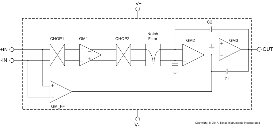
Table 2. Component Count
| COMPONENT | COUNT |
|---|---|
| Transistors | 636 |
| Diodes | 5 |
| Resistors | 41 |
| Capacitors | 72 |
8.3 Feature Description
The OPAx188-Q1 series is unity-gain stable and free from unexpected output phase reversal. This device series uses a proprietary, periodic zero-drift technique to provide low input offset voltage and very low input offset voltage drift over temperature. For lowest offset voltage and precision performance, optimize circuit layout and mechanical conditions. Avoid temperature gradients that create thermoelectric (Seebeck) effects in the thermocouple junctions formed from connecting dissimilar conductors. Cancel these thermally-generated potentials by ensuring the potentials are equal on both input pins. Other layout and design considerations include:
• Use low thermoelectric-coefficient conditions (avoid dissimilar metals).
• Thermally isolate components from power supplies or other heat sources.
• Shield the operational amplifier and input circuitry from air currents, such as cooling fans.
Follow these guidelines to reduce the likelihood of junctions being at different temperatures, which may cause thermoelectric voltages of 0.1 µV/°C or higher, depending on the materials used.
8.3.1 Operating Characteristics
The OPAx188-Q1 is specified for operation from 4 V to 36 V (±2 V to ±18 V). Many specifications apply from –40°C to +125°C. Parameters that can exhibit significant variance with regard to operating voltage or temperature are presented in Typical Characteristics.
8.3.2 Phase-Reversal Protection
The OPAx188-Q1 series has an internal phase-reversal protection. Many op amps exhibit a phase reversal when the input is driven beyond the linear common-mode range. This condition is most often encountered in noninverting circuits when the input is driven beyond the specified common-mode voltage range, causing the output to reverse into the opposite rail. The OPAx188-Q1 series input prevents phase reversal with excessive common-mode voltage. Instead, the output limits into the appropriate rail; Figure 38 shows this performance.
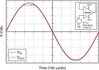 Figure 38. No Phase Reversal
8.3.3 Input Bias Current Clock Feedthrough
Zero-drift amplifiers (such as the OPAx188-Q1 series) use switching on the inputs to correct for the intrinsic offset and drift of the amplifier. Charge injection from the integrated switches on the inputs can introduce very short transients in the input bias current of the amplifier. The extremely short duration of these pulses prevents the devices from being amplified. However, the devices may be coupled to the output of the amplifier through the feedback network. The most effective method to prevent transients in the input bias current from producing additional noise at the amplifier output is to use a low-pass filter such as an RC network.
8.3.4 Internal Offset Correction
The OPAx188-Q1 op amp series uses an auto-calibration technique with a time-continuous 750-kHz op amp in the signal path. This amplifier is zero-corrected every 3 μs using a proprietary technique. Upon power up, the amplifier requires approximately 100 μs to achieve the specified VOS accuracy. This design has no aliasing or flicker noise.
8.3.5 EMI Rejection
The OPAx188-Q1 series uses integrated electromagnetic interference (EMI) filtering to reduce the effects of EMI interference from sources such as wireless communications and densely-populated boards with a mix of analog signal chain and digital components. EMI immunity can be improved with circuit design techniques; the OPAx188-Q1 series benefits from these design improvements. Texas Instruments™ has developed the ability to accurately measure and quantify the immunity of an operational amplifier over a broad frequency spectrum extending from 10 MHz to 6 GHz. Figure 39 shows the results of this testing on the OPAx188-Q1. Table 3 lists the EMIRR IN+ values for the OPAx188-Q1 devices at particular frequencies commonly encountered in real-world applications. Applications listed in Table 3 may be centered on or operated near the particular frequency shown. Detailed information can also be found in EMI Rejection Ratio of Operational Amplifiers, available for download from www.ti.com.
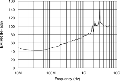 Figure 39. EMIRR Testing
Table 3. OPAx188-Q1 EMIRR IN+ for Frequencies of Interest
| FREQUENCY | APPLICATION OR ALLOCATION | EMIRR IN+ |
|---|---|---|
| 400 MHz | Mobile radio, mobile satellite, space operation, weather, radar, ultra-high frequency (UHF) applications | 62.2 dB |
| 900 MHz | Global system for mobile communications (GSM) applications, radio communication, navigation, GPS (to 1.6 GHz), GSM, aeronautical mobile, UHF applications | 74.7 dB |
| 1.8 GHz | GSM applications, mobile personal communications, broadband, satellite, L-band (1 GHz to 2 GHz) | 100.7 dB |
| 2.4 GHz | 802.11b, 802.11g, 802.11n, Bluetooth®, mobile personal communications, industrial, scientific and medical (ISM) radio band, amateur radio and satellite, S-band (2 GHz to 4 GHz) | 102.4 dB |
| 3.6 GHz | Radiolocation, aero communication and navigation, satellite, mobile, S-band | 104.8 dB |
| 5 GHz | 802.11a, 802.11n, aero communication and navigation, mobile communication, space and satellite operation, C-band (4 GHz to 8 GHz) | 100.3 dB |
8.3.6 Capacitive Load and Stability
The device dynamic characteristics are optimized for a range of common operating conditions. The combination of low closed-loop gain and high capacitive loads decreases the amplifier phase margin and can lead to gain peaking or oscillations. As a result, larger capacitive loads must be isolated from the output. The simplest way to achieve this isolation is to add a small resistor (for example, ROUT equal to 50 Ω) in series with the output. Figure 40 and Figure 41 show graphs of small-signal overshoot versus capacitive load for several values of ROUT. For details of analysis techniques and application circuits, see Feedback Plots Define Op Amp AC Performance, available for download from www.ti.com.
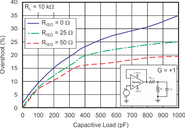
| G = 1 | RL = 10 kΩ | 100-mV Output Step |
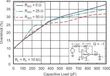
| G = –1 | RL = RF = 10 kΩ | 100-mV Output Step |
8.3.7 Electrical Overstress
Designers often ask questions about the capability of an operational amplifier to withstand electrical overstress. These questions tend to focus on the device inputs, but may involve the supply voltage pins or the output pin. Each of these different pin functions have electrical stress limits determined by the voltage breakdown characteristics of the particular semiconductor fabrication process and specific circuits connected to the pin. Additionally, internal electrostatic discharge (ESD) protection is built into these circuits to protect them from accidental ESD events both before and during product assembly.
Having a good understanding of this basic ESD circuitry and its relevance to an electrical overstress event is helpful. See Figure 42 for an illustration of the ESD circuits contained in the OPAx188-Q1 (indicated by the dashed line area). The ESD protection circuitry involves several current-steering diodes connected from the input and output pins and routed back to the internal power-supply lines, where the diodes meet at an internal absorption device of the operational amplifier. This protection circuitry is intended to remain inactive during normal circuit operation.
An ESD event produces a short-duration, high-voltage pulse that is transformed into a short-duration, high-current pulse while discharging through a semiconductor device. The ESD protection circuits are designed to provide a current path around the operational amplifier core to prevent damage. The energy absorbed by the protection circuitry is dissipated as heat.
When an ESD voltage develops across two or more amplifier device pins, current flows through one or more steering diodes. Depending on the path that the current takes, the absorption device may activate. The absorption device has a trigger, or threshold voltage, that is above the normal operating voltage of the
OPAx188-Q1 but below the device breakdown voltage level. When this threshold is exceeded, the absorption device quickly activates and clamps the voltage across the supply rails to a safe level.
When the operational amplifier connects into a circuit (such as Figure 42 shows), the ESD protection components are intended to remain inactive and do not become involved in the operation of the application circuit. However, circumstances may arise where an applied voltage exceeds the operating voltage range of a given pin. If this condition occurs, there is a risk that some internal ESD protection circuits may be biased on and conduct current. Any such current flow occurs through steering-diode paths and rarely involves the absorption device.
Figure 42 shows a specific example where the input voltage, VIN, exceeds the positive supply voltage (+VS) by 500 mV or more. Much of what happens in the circuit depends on the supply characteristics. If +VS can sink the current, one of the upper-input steering diodes conducts and directs current to +VS. Excessively high current levels can flow with increasingly higher VIN. As a result, the data sheet specifications recommend that applications limit the input current to 10 mA.
If the supply is not capable of sinking the current, VIN may begin sourcing current to the operational amplifier, and then take over as the source of positive supply voltage. The danger in this case is that the voltage can rise to levels that exceed the absolute maximum ratings of the operational amplifier.
Another common question involves what happens to the amplifier if an input signal is applied to the input while the power supplies (+VS or –VS) are at 0 V. Again, this question depends on the supply characteristic while at 0 V, or at a level below the input signal amplitude. If the supplies appear as high impedance, then the operational amplifier supply current may be supplied by the input source through the current-steering diodes. This state is not a normal bias condition; the amplifier will not operate normally. If the supplies are low impedance, then the current through the steering diodes can become quite high. The current level depends on the ability of the input source to deliver current, and any resistance in the input path.
If there is any uncertainty about the ability of the supply to absorb this current, external zener diodes may be added to the supply pins, as shown in Figure 42. The zener voltage must be selected such that the diode does not turn on during normal operation. However, the zener voltage must be low enough so that the zener diode conducts if the supply pin begins to rise above the safe operating supply voltage level.
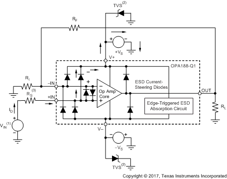
The OPAx188-Q1 series input terminals are protected from excessive differential voltage with back-to-back diodes, as shown in Figure 42. In most circuit applications, the input protection circuitry has no consequence. However, in low-gain and G = 1 circuits, fast-ramping input signals can forward-bias these diodes because the output of the amplifier cannot respond rapidly enough to the input ramp. If the input signal is fast enough to create this forward-bias condition, the input signal current must be limited to 10 mA or less. If the input signal current is not inherently limited, an input series resistor can be used to limit the signal input current. This input series resistor degrades the low-noise performance of the OPAx188-Q1 series. Figure 42 shows an example configuration that implements a current-limiting feedback resistor.
8.4 Device Functional Modes
The OPAx188-Q1 series has a single functional mode, and is operational when the power-supply voltage is greater than 4.5 V (±2.25 V). The maximum power supply voltage for the OPAx188-Q1 family is 36 V (±18 V).