SBOS860 April   2017 OPA188-Q1 , OPA2188-Q1

PRODUCTION DATA.  

  1. Features
  2. Applications
  3. Description
  4. Revision History
  5. Device Comparison Table
    1. 5.1 Portfolio Comparison
  6. Pin Configuration and Functions
  7. Specifications
    1. 7.1 Absolute Maximum Ratings
    2. 7.2 ESD Ratings
    3. 7.3 Recommended Operating Conditions
    4. 7.4 Thermal Information
    5. 7.5 Electrical Characteristics: High-Voltage Operation
    6. 7.6 Electrical Characteristics: Low-Voltage Operation
    7. 7.7 Typical Characteristics: Table of Graphs
      1. 7.7.1 Table of Graphs
    8. 7.8 Typical Characteristics
  8. Detailed Description
    1. 8.1 Overview
    2. 8.2 Functional Block Diagram
    3. 8.3 Feature Description
      1. 8.3.1 Operating Characteristics
      2. 8.3.2 Phase-Reversal Protection
      3. 8.3.3 Input Bias Current Clock Feedthrough
      4. 8.3.4 Internal Offset Correction
      5. 8.3.5 EMI Rejection
      6. 8.3.6 Capacitive Load and Stability
      7. 8.3.7 Electrical Overstress
    4. 8.4 Device Functional Modes
  9. Application and Implementation
    1. 9.1 Application Information
    2. 9.2 Typical Applications
      1. 9.2.1 High-Side Voltage-to-Current (V-I) Converter
        1. 9.2.1.1 Design Requirements
        2. 9.2.1.2 Detailed Design Procedure
        3. 9.2.1.3 Application Curves
      2. 9.2.2 Discrete INA + Attenuation for ADC With 3.3-V Supply
      3. 9.2.3 Bridge Amplifier
      4. 9.2.4 Low-Side Current Monitor
      5. 9.2.5 Programmable Power Supply
      6. 9.2.6 RTD Amplifier With Linearization
  10. 10Power Supply Recommendations
  11. 11Layout
    1. 11.1 Layout Guidelines
    2. 11.2 Layout Example
  12. 12Device and Documentation Support
    1. 12.1 Device Support
      1. 12.1.1 Development Support
        1. 12.1.1.1 TINA-TI (Free Download Software)
    2. 12.2 Documentation Support
      1. 12.2.1 Related Documentation
    3. 12.3 Related Links
    4. 12.4 Receiving Notification of Documentation Updates
    5. 12.5 Community Resources
    6. 12.6 Trademarks
    7. 12.7 Electrostatic Discharge Caution
    8. 12.8 Glossary
  13. 13Mechanical, Packaging, and Orderable Information

Package Options

Mechanical Data (Package|Pins)
Thermal pad, mechanical data (Package|Pins)
Orderable Information

Layout

Layout Guidelines

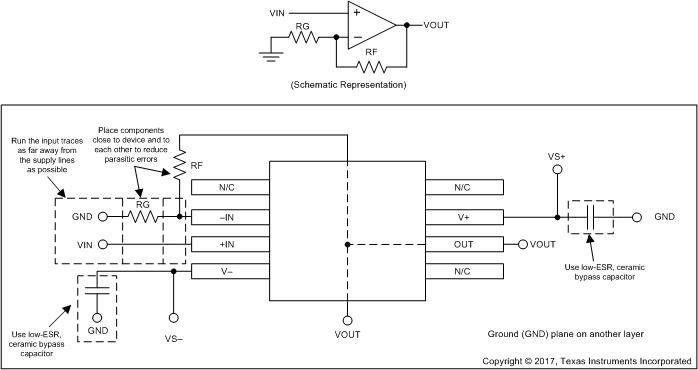
For best operational performance of the device, use good printed circuit board (PCB) layout practices, including:

  • Low-ESR, 0.1-µF ceramic bypass capacitors must be connected between each supply pin and ground, placed as close to the device as possible. A single bypass capacitor from V+ to ground is applicable to single-supply applications.
  • To reduce parasitic coupling, run the input traces as far away from the supply lines as possible.
  • A ground plane helps distribute heat and reduces EMI noise pickup.
  • Place the external components as close to the device as possible. This configuration prevents parasitic errors (such as the Seebeck effect) from occurring.
  • Consider a driven, low-impedance guard ring around the critical traces. A guard ring can significantly reduce leakage currents from nearby traces that are at different potentials.

Layout Example

OPA188-Q1 OPA2188-Q1 layout_example_sbos642.gif Figure 50. Layout Example