SBOS525C August 2011 – June 2016 OPA2188
PRODUCTION DATA.
- 1 Features
- 2 Applications
- 3 Description
- 4 Revision History
- 5 Zero-Drift Amplifier Portfolio
- 6 Pin Configuration and Functions
-
7 Specifications
- 7.1 Absolute Maximum Ratings
- 7.2 ESD Ratings
- 7.3 Recommended Operating Conditions
- 7.4 Thermal Information
- 7.5 Electrical Characteristics: High-Voltage Operation, VS = ±4 V to ±18 V (VS = 8 V to 36 V)
- 7.6 Electrical Characteristics: Low-Voltage Operation, VS = ±2 V to < ±4 V (VS = +4 V to < +8 V)
- 7.7 Typical Characteristics: Table of Graphs
- 7.8 Typical Characteristics
- 8 Detailed Description
- 9 Application and Implementation
- 10Power Supply Recommendations
- 11Layout
- 12Device and Documentation Support
- 13Mechanical, Packaging, and Orderable Information
Package Options
Mechanical Data (Package|Pins)
Thermal pad, mechanical data (Package|Pins)
- DGK|8
Orderable Information
1 Features
- Low Offset Voltage: 25 μV (Maximum)
- Zerø-Drift: 0.03 μV/°C
- Low Noise: 8.8 nV/√Hz
0.1-Hz to 10-Hz Noise: 0.25 µVPP - Excellent DC Precision:
PSRR: 142 dB
CMRR: 146 dB
Open-Loop Gain: 136 dB - Gain Bandwidth: 2 MHz
- Quiescent Current: 475 μA (Maximum)
- Wide Supply Range: ±2 V to ±18 V
- Rail-to-Rail Output:
Input Includes Negative Rail - RFI Filtered Inputs
- MicroSIZE Packages
2 Applications
3 Description
The OPA2188 operational amplifier uses TI proprietary auto-zeroing techniques to provide low offset voltage (25 μV, maximum), and near zero-drift over time and temperature. This miniature, high-precision, low quiescent current amplifier offers high input impedance and rail-to-rail output swing within 15 mV of the rails. The input common-mode range includes the negative rail. Either single or dual supplies can be used in the range of 4 V to 36 V (±2 V to ±18 V).
The OPA2188 device is available in MSOP-8 and SO-8 packages. The device is specified for operation from –40°C to +105°C.
Device Information(1)
| PART NUMBER | PACKAGE | BODY SIZE (NOM) |
|---|---|---|
| OPA2188 | SOIC (8) | 4.90 mm × 3.91 mm |
| VSSOP (8) | 3.00 mm × 3.00 mm |
- For all available packages, see the orderable addendum at the end of the data sheet.
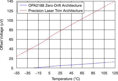
Offset Voltage vs Temperature
