SBOS483I July 2009 – May 2015 OPA2333-HT
PRODUCTION DATA.
- 1 Features
- 2 Applications
- 3 Description
- 4 Revision History
- 5 Pin Configuration and Functions
- 6 Specifications
- 7 Detailed Description
- 8 Application and Implementation
- 9 Power Supply Recommendations
- 10Layout
- 11Device and Documentation Support
- 12Mechanical, Packaging, and Orderable Information
Package Options
Mechanical Data (Package|Pins)
Thermal pad, mechanical data (Package|Pins)
Orderable Information
1 Features
- Low Offset Voltage: 26 μV (Maximum)
- 0.01-Hz to 10-Hz Noise: 1.5 μVPP
- Quiescent Current: 50 μA
- Single-Supply Operation
- Supply Voltage: 1.8 V to 5.5 V
- Rail-to-Rail Input and Output
- Supports Extreme Temperature Applications
- Controlled Baseline
- One Assembly/Test Site
- One Fabrication Site
- Available in Extreme (–55°C to 210°C) Temperature Range
- Extended Product Life Cycle
- Extended Product-Change Notification
- Product Traceability
- Texas Instruments' high temperature products use highly optimized silicon (die) solutions with design and process enhancements to maximize performance over extended temperatures.
2 Applications
- Down-Hole Drilling
- High Temperature Environments
3 Description
The OPA2333 series of CMOS operational amplifiers uses a proprietary auto-calibration technique to simultaneously provide very low offset voltage and near-zero drift over time and temperature(1). These miniature, high-precision, low-quiescent-current amplifiers offer high-impedance inputs that have a common-mode range 100 mV beyond the rails, and rail-to-rail output that swings within 150 mV of the rails. Single or dual supplies as low as 1.8 V (±0.9 V) and up to 5.5 V (±2.75 V) may be used. They are optimized for low-voltage single-supply operation.
The OPA2333 offers excellent common-mode rejection ratio (CMRR) without the crossover associated with traditional complementary input stages. This design results in superior performance for driving analog-to-digital converters (ADCs) without degradation of differential linearity.
Device Information(2)
| PART NUMBER | PACKAGE | BODY SIZE (NOM) |
|---|---|---|
| OPA2333-HT | SOIC (8) | 4.90 mm × 3.91 mm |
| CFP (8) | 6.90 mm × 5.65 mm | |
| CFP (8) | 7.035 mm × 5.75 mm | |
| CDIP SB (8) | 18.55 mm × 7.49 mm |
- See Electrical Characteristics for
performance degradation over temperature. - For all available packages, see the orderable addendum at the end of the data sheet.
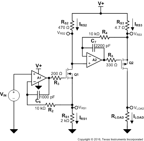
Typical Application
