SLOS856B June 2013 – May 2017 OPA2322-Q1 , OPA322-Q1 , OPA4322-Q1
PRODUCTION DATA.
- 1 Features
- 2 Applications
- 3 Description
- 4 Revision History
- 5 Pin Configuration and Functions
- 6 Specifications
- 7 Typical Characteristics
- 8 Detailed Description
- 9 Application and Implementation
- 10Power Supply Recommendations
- 11Layout
- 12Device and Documentation Support
- 13Mechanical, Packaging, and Orderable Information
Package Options
Mechanical Data (Package|Pins)
- DBV|5
Thermal pad, mechanical data (Package|Pins)
Orderable Information
9 Application and Implementation
NOTE
Information in the following applications sections is not part of the TI component specification, and TI does not warrant its accuracy or completeness. TI’s customers are responsible for determining suitability of components for their purposes. Customers should validate and test their design implementation to confirm system functionality.
9.1 Application Information
The OPAx322-Q1 family offers outstanding DC and AC performance. These devices operate up to a 5.5-V power supply and offer ultra-low input bias current and 20-MHz bandwidth. These features make the OPAx322-Q1 family a robust operational amplifier for both battery-powered and industrial applications.
9.1.1 Active Filter
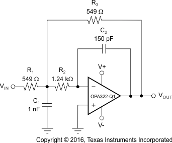
The OPAx322-Q1 is well-suited for active filter applications that require a wide bandwidth, fast slew rate, low-noise, single-supply operational amplifier. Figure 33 shows a 500-kHz, second-order, low-pass filter using the multiple-feedback (MFB) topology. The components are selected to provide a maximally flat Butterworth response. Beyond the cutoff frequency, roll-off is –40 dB/dec. The Butterworth response is ideal for applications that require predictable gain characteristics, such as the anti-aliasing filter used in front of an ADC.
One point to observe when considering the MFB filter is that the output is inverted relative to the input. If this inversion is not required (or not desired) a noninverting output can be achieved through one of these options:
- Adding an inverting amplifier
- Adding an additional second-order MFB stage
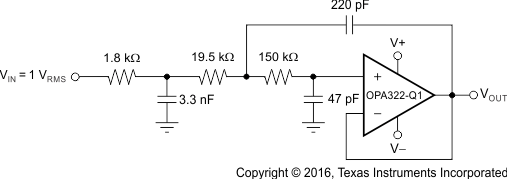
- Using a noninverting filter topology, such as the Sallen-Key (shown in Figure 34).
MFB, Sallen-Key, low-pass, and high-pass filter synthesis is quickly accomplished using TI’s FilterPro™ program. This software is available as a free download at www.ti.com.
 Figure 33. Second-Order, Butterworth, 500-kHz Low-Pass Filter
 Figure 34. OPAx322-Q1 Configured as a Three-Pole, 20-kHz, Sallen-Key Filter
9.2 Typical Application
9.2.1 Design Requirements
- Gain = 1 V/V
- Low-pass cutoff frequency = 50 kHz
- –40-db/dec filter response
- Maintain less than 3-dB gain peaking in the gain versus frequency response
9.2.2 Detailed Design Procedure
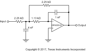
The infinite-gain multiple-feedback circuit for a low-pass network function is shown in Equation 2. Use Equation 2 to calculate the voltage transfer function.

This circuit produces a signal inversion. For this circuit, the gain at DC and the low-pass cutoff frequency are calculated by Equation 3.

Software tools are readily available to simplify filter design. WEBENCH® Filter Designer is a simple, powerful, and easy-to-use active filter design program. The WEBENCH® Filter Designer allows the user to create optimized filter designs using a selection of TI operational amplifiers and passive components from TI's vendor partners.
Available as a web-based tool from the WEBENCH® Design Center, WEBENCH® Filter Designer allows the user to design, optimize, and simulate complete multistage active filter solutions within minutes.
9.2.3 Application Curve
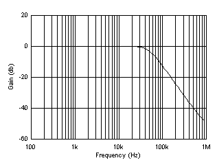
 Figure 36. OPAx322-Q1 Second-Order, 50-kHz, Low-Pass Filter
