SBOS099D September 2000 – December 2015 OPA2350 , OPA350 , OPA4350
PRODUCTION DATA.
- 1 Features
- 2 Applications
- 3 Description
- 4 Revision History
- 5 Pin Configuration and Functions
- 6 Specifications
- 7 Detailed Description
-
8 Application and Implementation
- 8.1 Application Information
- 8.2 Typical Applications
- 9 Power Supply Recommendations
- 10Layout
- 11Device and Documentation Support
- 12Mechanical, Packaging, and Orderable Information
Package Options
Mechanical Data (Package|Pins)
Thermal pad, mechanical data (Package|Pins)
Orderable Information
1 Features
2 Applications
- Cell Phone PA Control Loops
- Driving A/D Converters
- Video Processing
- Data Acquisition
- Process Controls
- Audio Processing
- Communications
- Active Filters
- Test Equipment
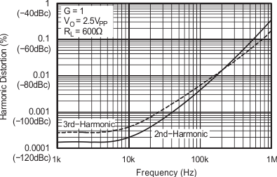
OPAx350 Harmonic Distortion

3 Description
The OPA350 series of rail-to-rail CMOS operational amplifiers are optimized for low voltage, single-supply operation. Rail-to-rail input and output, low noise (5 nV/√Hz), and high speed operation (38 MHz, 22 V/μs) make the amplifiers ideal for driving sampling Analog-to-Digital (A/D) converters. They are also suited for cell phone PA control loops and video processing (75-Ω drive capability), as well as audio and general purpose applications. Single, dual, and quad versions have identical specifications for maximum design flexibility.
The OPA350 series operates on a single supply as low as 2.5 V, with an input common-mode voltage range that extends 300 mV below ground and 300 mV above the positive supply. Output voltage swing is to within 10 mV of the supply rails, with a 10-kΩ load. Dual and quad designs feature completely independent circuitry for lowest crosstalk and freedom from interaction.
The single (OPA350) and dual (OPA2350) come in the miniature MSOP-8 surface mount, SO-8 surface mount, and DIP-8 packages. The quad (OPA4350) packages are in the space-saving SSOP-16 surface mount and SO-14 surface mount. All are specified from −40°C to 85°C and operate from −55°C to 150°C.
Device Information(1)
| PART NUMBER | PACKAGE | BODY SIZE (NOM) |
|---|---|---|
| OPA350 | MSOP (8) | 3.00 mm × 3.00 mm |
| SOIC (8) | 3.91 mm × 4.90 mm | |
| PDIP (8) | 6.35 mm × 9.81 mm | |
| OPA2350 | MSOP (8) | 3.00 mm × 3.00 mm |
| SOIC (8) | 3.91 mm × 4.90 mm | |
| PDIP (8) | 6.35 mm × 9.81 mm | |
| OPA4350 | SSOP (16) | 3.90 mm × 4.90 mm |
| SOIC (14) | 3.91 mm × 8.65 mm |
- For all available packages, see the orderable addendum at the end of the data sheet.
4 Revision History
Changes from C Revision (January 2005) to D Revision
- Added ESD Ratings table, Feature Description section, Device Functional Modes, Application and Implementation section, Power Supply Recommendations section, Layout section, Device and Documentation Support section, and Mechanical, Packaging, and Orderable Information section. Go