SBOS197F December 2001 – August 2015 OPA657
PRODUCTION DATA.
- 1 Features
- 2 Applications
- 3 Description
- 4 Revision History
- 5 Related Operational Amplifier Products
- 6 Pin Configuration and Functions
- 7 Specifications
- 8 Detailed Description
- 9 Application and Implementation
- 10Power Supply Recommendations
- 11Layout
- 12Device and Documentation Support
- 13Mechanical, Packaging, and Orderable Information
Package Options
Mechanical Data (Package|Pins)
Thermal pad, mechanical data (Package|Pins)
Orderable Information
9 Application and Implementation
NOTE
Information in the following applications sections is not part of the TI component specification, and TI does not warrant its accuracy or completeness. TI’s customers are responsible for determining suitability of components for their purposes. Customers should validate and test their design implementation to confirm system functionality.
9.1 Application Information
9.1.1 Wideband, Noninverting Operation
The OPA657 provides a unique combination of low-input voltage noise, very high-gain bandwidth, and the DC precision of a trimmed JFET-input stage to give an exceptional high input impedance, high-gain stage amplifier. Its very high gain bandwidth product (GBP) can be used to either deliver high-signal bandwidths at high gains, or to extend the achievable bandwidth or gain in photodiode-transimpedance applications. To achieve the full performance of the OPA657, careful attention to printed circuit board (PCB) layout and component selection is required as discussed in the following sections of this data sheet.
Figure 29 shows the noninverting gain of +10-V/V circuit used as the basis for most of the Typical Characteristics: VS = ±5 V. Most of the curves are characterized using signal sources with 50-Ω driving impedance, and with measurement equipment presenting a 50-Ω load impedance. In Figure 29, the 50-Ω shunt resistor at the VI terminal matches the source impedance of the test generator, while the 50-Ω series resistor at the VO terminal provides a matching resistor for the measurement equipment load. Generally, data sheet voltage swing specifications are at the output pin (VO in Figure 29) while output power specifications are at the matched 50-Ω load. The total 100-Ω load at the output combined with the 500-Ω total feedback network load presents the OPA657 with an effective output load of 83 Ω for the circuit of Figure 29.
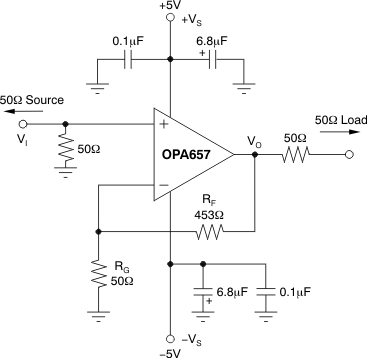 Figure 29. Noninverting G = +10 V/V Specifications and Test Circuit
Voltage-feedback operational amplifiers, unlike current-feedback amplifiers, can use a wide range of resistor values to set the gain. To retain a controlled frequency response for the noninverting voltage amplifier of Figure 29, the parallel combination of RF || RG should always be less than 150 Ω. In the noninverting configuration, the parallel combination of RF || RG forms a pole with the parasitic input capacitance at the inverting node of the OPA657 (including layout parasitics). For best performance, this pole should be at a frequency greater than the closed-loop bandwidth for the OPA657. For lower noninverting gains than the minimum recommended gain of +7 for the OPA657, consider the unity-gain stable JFET input OPA656 or high slew rate, low gain stable OPA659.
9.1.2 Wideband, Inverting Gain Operation
There can be significant benefits to operating the OPA657 as an inverting amplifier. This is particularly true when a matched input impedance is required. Figure 30 shows the inverting gain circuit used as a starting point for the Typical Characteristics showing inverting-mode performance.
Driving this circuit from a 50-Ω source, and constraining the gain resistor (RG) to equal 50 Ω gives both a signal bandwidth and noise advantage. RG in this case is acting as both the input termination resistor and the gain setting resistor for the circuit. Although the signal gain for the circuit of Figure 30 is double that for Figure 29, the noise gains are equal when the 50-Ω source resistor is included. This has the interesting effect of doubling the equivalent GBP for the amplifier. This can be seen in comparing the G = +10 V/V and G = –20 V/V small-signal frequency response curves. Both show about 250-MHz bandwidth, but the inverting configuration of Figure 30 is giving 6-dB higher signal gain. If the signal source is actually the low-impedance output of another amplifier, RG should be increased to the minimum value allowed at the output of that amplifier and RF adjusted to get the desired gain. It is critical for stable operation of the OPA657 that this driving amplifier show a very low output impedance through frequencies exceeding the expected closed-loop bandwidth for the OPA657.
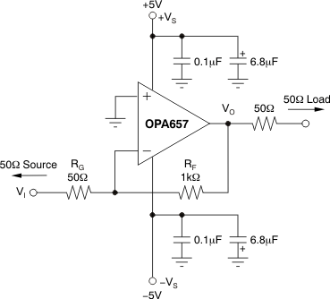 Figure 30. Inverting G = –20 V/V Specifications and Test Circuit
Figure 30 also shows the noninverting input tied directly to ground. Often, a bias current canceling resistor to ground is included here to null out the DC errors caused by the input bias currents. This is only useful when the input bias currents are matched. For a JFET part like the OPA657, the input bias currents do not match but are so low to begin with (< 5 pA) that DC errors as a result of input bias currents are negligible. Hence, no resistor is recommended at the noninverting input for the inverting signal gain condition.
9.1.3 Low-Gain Compensation
Where a low gain is desired, and inverting operation is acceptable, a new external compensation technique may be used to retain the full slew rate and noise benefits of the OPA657 while maintaining the increased loop gain and the associated improvement in distortion offered by the decompensated architecture. This technique shapes the loop gain for good stability while giving an easily-controlled second-order low-pass frequency response. Considering only the noise gain for the circuit of Figure 31, the low-frequency noise gain, (NG1) is set by the resistor ratios while the high frequency noise gain (NG2) is set by the capacitor ratios. The capacitor values set both the transition frequencies and the high-frequency noise gain. If this noise gain, determined by NG2 = 1 + CS/CF, is set to a value greater than the recommended minimum stable gain for the operational amplifier and the noise gain pole, set by 1/RFCF, is placed correctly, a very well controlled second-order low-pass frequency response results.
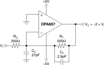 Figure 31. Broadband Low-Gain Inverting External Compensation
To choose the values for both CS and CF, two parameters and only three equations must be solved. The first parameter is the target high-frequency noise gain NG2, which should be greater than the minimum stable gain for the OPA657. Here, a target NG2 of 10.5 V/V is used. The second parameter is the desired low-frequency signal gain, which also sets the low-frequency noise gain NG1. To simplify this discussion, target a maximally-flat second-order low-pass Butterworth frequency response (Q = 0.707). The signal gain of –2 V/V shown in Figure 31 sets the low-frequency noise gain to NG1 = 1 + RF/RG (= 3 in this example). Then, using only these two gains and the GBP for the OPA657 (1600 MHz), the key frequency in the compensation can be determined as:

Physically, this ZO (10.6 MHz for the values shown above) is set by 1/(2π × RF(CF + CS)) and is the frequency at which the rising portion of the noise gain would intersect unity gain if projected back to 0-dB gain. The actual zero in the noise gain occurs at NG1 × ZO and the pole in the noise gain occurs at NG2 × ZO. Because GBP is expressed in Hz, multiply ZO by 2π and use this to get CF by solving:

Finally, because CS and CF set the high-frequency noise gain, determine CS by using [NG2 = 10.5]:

The resulting closed-loop bandwidth is approximately equal to:

For the values shown in Figure 31, the f–3 dB is approximately 130 MHz. This is less than that predicted by simply dividing the GBP product by NG1. The compensation network controls the bandwidth to a lower value while providing the full slew rate at the output and an exceptional distortion performance due to increased loop gain at frequencies below NG1 × ZO. The capacitor values shown in Figure 31 are calculated for NG1 = 3 and NG2 = 10.5 with no adjustment for parasitics.
Figure 32 shows the gain of –2 V/V (6 dB) measured frequency response for the circuit of Figure 31. The amplifier displays exceptional gain flatness through 70 MHz and a –3-dB bandwidth of 170 MHz.
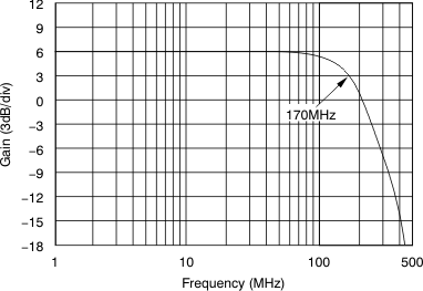 Figure 32. G = –2 Frequency Response With External Compensation
The real benefit to this compensation is to allow a high slew rate, exceptional DC precision operational amplifier to provide a low overshoot, fast settling pulse response. For a 1-V output step, the 700-V/μs slew rate of the OPA657 allows a rise time limited edge rate (2ns for a 170-MHz bandwidth). While unity-gain stable operational amplifiers may offer comparable bandwidths, the lower slew rates extend the settling time for larger steps. For instance, the OPA656 can also provide a 150-MHz gain of –2-V/V bandwidth implying a 2.3-ns transition time. However, the lower slew rate of this unity-gain stable amplifier (290 V/μs) limits a 1-V step transition to 3.5 ns and delays the settling time as the slewing transition is recovered. The combination of higher slew rate and exceptional DC precision for the OPA657 can yield one of the fastest, most precise, pulse amplifiers using the circuit of Figure 31.
An added benefit to the compensation of Figure 31 is to increase the loop gain above that achievable at comparable gains by internally-compensated amplifiers. The circuit of Figure 31 has lower harmonic distortion through 10 MHz than the OPA656 operated at a gain of –2 V/V.
9.1.4 Operating Suggestions
9.1.4.1 Setting Resistor Values to Minimize Noise
The OPA657 provides a very low input noise voltage while requiring a low 14 mA of quiescent current. To take full advantage of this low input noise, careful attention to the other possible noise contributors is required. Figure 33 shows the operational amplifier noise analysis model with all the noise terms included. In this model, all the noise terms are taken to be noise voltage or current density terms in either nV/√Hz or pA/√Hz.
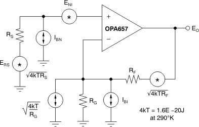 Figure 33. Operational Amplifier Noise Analysis Model
The total output spot noise voltage can be computed as the square root of the squared contributing terms to the output noise voltage. This computation is adding all the contributing noise powers at the output by superposition, then taking the square root to get back to a spot noise voltage. Equation 5 shows the general form for this output noise voltage using the terms shown in Figure 28:

Dividing this expression by the noise gain (GN = 1 + RF/RG) gives the equivalent input referred spot noise voltage at the noninverting input, as shown in Equation 6:

Putting high resistor values into Equation 6 can quickly dominate the total equivalent input referred noise. A source impedance on the noninverting input of 1.6 kΩ adds a Johnson voltage noise term equal to just that for the amplifier itself (5 nV/√Hz). While the JFET input of the OPA657 is ideal for high source impedance applications, both the overall bandwidth and noise may be limited by these higher source impedances in the noninverting configuration of Figure 29.
9.1.4.2 Frequency Response Control
Voltage-feedback operational amplifiers exhibit decreasing closed-loop bandwidth as the signal gain is increased. In theory, this relationship is described by the gain bandwidth product (GBP) shown in the Electrical Characteristics: VS = ±5 V. Ideally, dividing GBP by the noninverting signal gain (also called the noise gain, or NG) predicts the closed-loop bandwidth. In practice, this only holds true when the phase margin approaches 90°, as it does in high-gain configurations. At low gains (increased feedback factors), most high-speed amplifiers exhibit a more complex response with lower phase margin. The OPA657 is compensated to give a maximally-flat, second-order, Butterworth, closed-loop response at a noninverting gain of +10 V/V (see Figure 29). This results in a typical gain of +10-V/V bandwidth of 275 MHz, far exceeding that predicted by dividing the 1600-MHz GBP by 10. Increasing the gain causes the phase margin to approach 90° and the bandwidth to more closely approach the predicted value of (GBP/NG). At a gain of +50 V/V the OPA657 shows the 32-MHz bandwidth predicted using the simple formula and the typical GBP of 1600 MHz. Inverting operation offers some interesting opportunities to increase the available gain-bandwidth product. When the source impedance is matched by the gain resistor (see Figure 30), the signal gain is –(RF/RG) while the noise gain for bandwidth purposes is (1 + RF/RG). This cuts the noise gain in half, increasing the minimum stable gain for inverting operation under these conditions to –12 V/V and the equivalent gain bandwidth product to 3.2 GHz.
9.1.4.3 Driving Capacitive Loads
One of the most demanding and yet very common load conditions for an operational amplifier is capacitive loading. Often, the capacitive load is the input of an ADC—including additional external capacitance which may be recommended to improve A/D linearity. A high-speed, high open-loop gain amplifier such as the OPA657 can be very susceptible to decreased stability and closed-loop response peaking when a capacitive load is placed directly on the output pin. When the amplifier open-loop output resistance is considered, this capacitive load introduces an additional pole in the signal path that can decrease the phase margin. Several external solutions to this problem have been suggested. When the primary considerations are frequency response flatness, pulse response fidelity, and/or distortion, the simplest and most effective solution is to isolate the capacitive load from the feedback loop by inserting a series isolation resistor between the amplifier output and the capacitive load. This does not eliminate the pole from the loop response, but rather shifts it and adds a zero at a higher frequency. The additional zero acts to cancel the phase lag from the capacitive load pole, thus increasing the phase margin and improving stability.
The Typical Characteristics illustrate the Recommended RS vs Capacitive Load (Figure 17) and the resulting frequency response at the load. In this case, a design target of a maximally-flat frequency response is used. Lower values of RS may be used if some peaking can be tolerated. Also, operating at higher gains (than the +10 V/V used in the Typical Characteristics) require lower values of RS for a minimally-peaked frequency response. Parasitic capacitive loads greater than 2 pF can begin to degrade the performance of the OPA657. Long PC board traces, unmatched cables, and connections to multiple devices can easily cause this value to be exceeded. Always consider this effect carefully, and add the recommended series resistor as close as possible to the OPA657 output pin (see the Layout Guidelines section).
9.1.4.4 Distortion Performance
The OPA657 is capable of delivering a low-distortion signal at high frequencies over a wide range of gains. The distortion plots in the Typical Characteristics: VS = ±5 V show the typical distortion under a wide variety of conditions.
Generally, until the fundamental signal reaches very high frequencies or powers, the second-harmonic dominates the distortion with a negligible third-harmonic component. Focusing then on the second-harmonic, increasing the load impedance improves distortion directly. Remember that the total load includes the feedback network—in the noninverting configuration this is sum of RF + RG, while in the inverting configuration this is just RF (see Figure 29). Increasing output voltage swing increases harmonic distortion directly. A 6-dB increase in output swing generally increases the second-harmonic 12 dB and the third-harmonic 18 dB. Increasing the signal gain also increases the second-harmonic distortion. Again, a 6-dB increase in gain increases the second- and third-harmonic by approximately 6 dB, even with a constant output power and frequency. And finally, the distortion increases as the fundamental frequency increases due to the roll-off in the loop gain with frequency. Conversely, the distortion improves going to lower frequencies down to the dominant open-loop pole at approximately 100 kHz. Starting from the –70-dBc second-harmonic for a 5-MHz, 2 VPP fundamental into a 200-Ω load at G = +10 V/V (from the Typical Characteristics: VS = ±5 V), the second-harmonic distortion for frequencies lower than 100 kHz is approximately less than –90 dBc.
The OPA657 has an extremely low third-order harmonic distortion. This also shows up in the two-tone, third-order, intermodulation spurious (IM3) response curves. The third-order spurious levels are extremely low (< –80 dBc) at low output power levels. The output stage continues to hold them low even as the fundamental power reaches higher levels. As shown in Typical Characteristics: VS = ±5 V, the spurious intermodulation powers do not increase as predicted by a traditional intercept model. As the fundamental power level increases, the dynamic range does not decrease significantly. For two tones centered at 10 MHz, with 4 dBm/tone into a matched 50-Ω load (that is, 1 VPP for each tone at the load, which requires 4 VPP for the overall two-tone envelope at the output pin), the Typical Characteristics: VS = ±5 V show a 82-dBc difference between the test tone and the third-order intermodulation spurious levels. This exceptional performance improves further when operating at lower frequencies and/or higher load impedances.
9.1.4.5 DC Accuracy and Offset Control
The OPA657 can provide excellent DC accuracy due to its high open-loop gain, high common-mode rejection, high power-supply rejection, and its trimmed input offset voltage (and drift) along with the negligible errors introduced by the low input bias current. For the best DC precision, a high-grade version (OPA657UB or OPA657NB) screens the key DC parameters to an even tighter limit. Both standard- and high-grade versions take advantage of a new final test technique to 100% test input offset voltage drift over temperature. This discussion uses the high-grade typical and min/max Electrical Characteristics: VS = ±5 V for illustration; however, an identical analysis applies to the standard-grade version.
The total output DC offset voltage in any configuration and temperature is the combination of a number of possible error terms. In a JFET part such as the OPA657, the input bias current terms are typically quite low but are unmatched. Using bias-current cancellation techniques, more typical in bipolar input amplifiers, does not improve output DC offset errors. Errors due to the input bias current only become dominant at elevated temperatures. The OPA657 shows the typical 2× increase in every 10°C common to JFET-input stage amplifiers. Using the 5-pA maximum tested value at +25°C, and a +20°C internal self heating (see thermal analysis), the maximum input bias current at +85°C ambient is 5 pA × 2(105 – 25)/10 = 1280 pA. For noninverting configurations, this term only begins to be a significant term versus the input offset voltage for source impedances greater than 750 kΩ. This would also be the feedback resistor value for transimpedance applications (see Figure 34) where the output DC error due to inverting input bias current is on the order of that contributed by the input offset voltage. In general, except for these extremely high-impedance values, the output DC errors due to the input bias current may be neglected.
After the input offset voltage itself, the most significant term contributing to output offset voltage is the PSRR for the negative supply. This term is modeled as an input offset voltage shift due to changes in the negative power-supply voltage (and similarly for the +PSRR). The high-grade test limit for –PSRR is 68 dB. This translates into 0.4-mV/V input offset voltage shift = 10(–68/20). This low sensitivity to the negative supply voltage requires a 1.5-V change in the negative supply to match the ±0.6mV input offset voltage error. The +PSRR is tested to a minimum value of 78 dB. This translates into 10(–78/20) = 0.125 mV/V sensitivity for the input offset voltage to positive power-supply changes.
As an example, compute the worst-case output DC error for the transimpedance circuit of Figure 34 at 25°C and then the shift over the 0°C to 70°C range given the following assumptions.
Negative Power Supply
= –5 V ±0.2 V with a ±5 mV/°C worst-case shift
Positive Power Supply
= +5 V ±0.2 V with a ±5 mV/°C worst-case shift
Initial 25°C Output DC Error Band
= ±0.6 mV (OPA657 high-grade input offset voltage limit)
±0.08 mV (due to the –PSRR = 0.4 mV/V × ±0.2 V)
±0.04 mV (due to the +PSRR = 0.2 mV/V × ±0.2 V)
Total = ±0.72mV
This would be the worst-case error band in volume production at 25°C acceptance testing given the conditions stated. Over the temperature range (0°C to 70°C), expect the following worst-case shifting from initial value. A 20°C internal junction self-heating is assumed here.
±0.36 mV (OPA657 high-grade input offset drift)
= ±6 μV/°C × (70°C + 20°C – 25°C)
±0.11 mV (–PSRR of 66dB with 5mV × (70°C – 25°C) supply shift)
±0.04 mV (+PSRR of 76dB with 5mV × (70°C – 25°C) supply shift)
Total = ±0.51mV
This would be the worst-case shift from an initial offset over a 0°C to 70°C ambient for the conditions stated. Typical initial output DC error bands and shifts over temperature are much lower than these worst-case estimates.
In the transimpedance configuration, the CMRR errors can be neglected because the input common-mode voltage is held at ground. For noninverting gain configurations (see Figure 29), the CMRR term needs to be considered but is typically far lower than the input offset voltage term. With a tested minimum of 91 dB (28 μV/V), the added apparent DC error is no more than ±0.06 mV for a ±2-V input swing to the circuit of Figure 29.
9.2 Typical Application
The high GBP and low input voltage and current noise for the OPA657 make it an ideal wideband transimpedance amplifier for moderate to high transimpedance gains. Unity-gain stability in the operational amplifier is not required for application as a transimpedance amplifier.
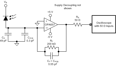 Figure 34. Wideband, High-Sensitivity, Transimpedance Amplifier Diagram
9.2.1 Design Requirements
Design a high-bandwidth, high-gain transimpedance amplifier with the design requirements shown in Table 1.
Table 1. Design Requirements
| TARGET BANDWIDTH (MHz) | TRANSIMPEDANCE GAIN (kΩ) | PHOTODIODE CAPACITANCE (pF) | |||
|---|---|---|---|---|---|
| 1 | 200 | 49 | |||
9.2.2 Detailed Design Procedure
Designs that require high bandwidth from a large area detector with relatively high transimpedance gain benefit from the low input voltage noise of the OPA657. This input voltage noise is peaked up over frequency by the diode source capacitance, and can, in many cases, become the limiting factor to input sensitivity. The key elements to the design are the expected diode capacitance (CD) with the reverse bias voltage (VB) applied, the desired transimpedance gain, RF, and the GBP for the OPA657 (1600 MHz). Figure 34 shows a transimpedance circuit with the parameters as described in Table 1. With these three variables set (and including the parasitic input capacitance for the OPA657 and the PCB added to CD), the feedback capacitor value (CF) may be set to control the frequency response. To achieve a maximally-flat second-order Butterworth frequency response, the feedback pole should be set to:

Adding the common-mode and differential mode input capacitance (0.7 + 4.5) pF and the trace PCB capacitance of approximately 0.3 pF to the 49-pF diode source capacitance of Figure 34, and targeting a 200-kΩ transimpedance gain using the 1600-MHz GBP for the OPA657 requires a feedback pole set to 3.5 MHz. This requires a total feedback capacitance of 0.2 pF. Such low capacitance values are difficult to achieve due to parasitics from the PCB and the surface mount components.
Equation 8 gives the approximate closed loop bandwidth of the system to be 4.8 MHz. Because the target bandwidth is only 1 MHz, the feedback capacitance can be increased to a more practical value while maintaining the bandwidth requirements of the design. A feedback capacitance of 0.550 pf was chosen. This includes the physical 0.4-pF feedback capacitor in addition to the 0.1-pF parasitic capacitance from the feedback resistor and around 50-fF capacitance from the PCB traces. Removing the ground and power planes from under the surface mount components helps to minimize this parasitic capacitance. The simulated closed loop bandwidth of Figure 34 was 1.7 MHz. The phase margin was close to 82°. This design should result in a system with negligible overshoot to a pulsed input.

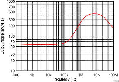
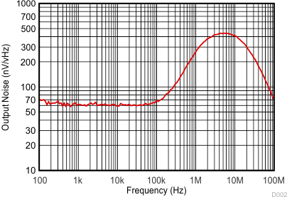
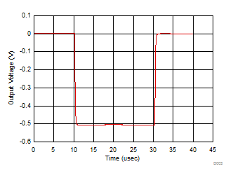
Figure 35 shows the measured output noise of the system which matches the simulated output noise in Figure 36 very closely. The low-frequency output noise of 60 nV/√Hz gets input-referred to 0.3 pA/√Hz. The transimpedance gain resistor is the dominant noise source with the operational amplifier itself contributing a negligible amount, reflecting one of the main benefits in using a JFET input amplifier in a high-gain transimpedance application. If the total output noise of the TIA is bandlimited to a frequency less than the feedback pole frequency, a very simple expression for the equivalent output noise voltage can be derived as: see Equation 9. Figure 37 shows the measured pulse response to a 5-µA input current pulse. The output voltage measured on the scope is 0.5 V because of the 50-Ω termination to the scope.

where
- VOUTN = Equivalent output noise when band limited to F < 1 / (2ΩRfCf)
- IN = Input current noise for the operational amplifier inverting input
- EN = Input voltage noise for the operational amplifier
- CD = Diode capacitance including operational amplifier and PCB parasitic capacitance
- F = Band-limiting frequency in Hz (usually a postfilter before further signal processing)
- 4 kT = 1.6 e – 20 J at T = 290°K
9.2.3 Application Curves
| Rise Time = 239 ns | Fall Time = 224 ns |
