SBOS197F December 2001 – August 2015 OPA657
PRODUCTION DATA.
- 1 Features
- 2 Applications
- 3 Description
- 4 Revision History
- 5 Related Operational Amplifier Products
- 6 Pin Configuration and Functions
- 7 Specifications
- 8 Detailed Description
- 9 Application and Implementation
- 10Power Supply Recommendations
- 11Layout
- 12Device and Documentation Support
- 13Mechanical, Packaging, and Orderable Information
Package Options
Mechanical Data (Package|Pins)
Thermal pad, mechanical data (Package|Pins)
Orderable Information
8 Detailed Description
8.1 Overview
The OPA657 is high gain-bandwidth, voltage feedback operational amplifier featuring a low noise JFET input stage. The OPA657 has been decompensated to allow for optimized Bandwidth to Quiescent current performance and better optimize its voltage noise performance. The OPA657 finds wide use in optical front-end applications and in test and measurement systems that require high input impedance. It is built using a very high speed complementary bipolar process.
8.2 Feature Description
8.2.1 Input and ESD Protection
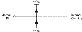
The internal junction breakdown voltages are relatively low for these very small geometry devices. These breakdowns are reflected in the Absolute Maximum Ratings table. All device pins are protected with internal ESD protection diodes to the power supplies, as shown in Figure 28.
These diodes provide moderate protection to input overdrive voltages above the supplies as well. The protection diodes can typically support 30-mA continuous current. Where higher currents are possible (that is, in systems with ±12-V supply parts driving into the OPA657), current limiting series resistors should be added into the two inputs. Keep these resistor values as low as possible because high values degrade both noise performance and frequency response.
 Figure 28. Internal ESD Protection
8.3 Device Functional Modes
8.3.1 Split-Supply Operation (±4-V to ±6-V)
To facilitate testing with common lab equipment, the OPA657 may be configured to allow for split-supply operation. This configuration eases lab testing because the mid-point between the power rails is ground, and most signal generators, network analyzers, oscilloscopes, spectrum analyzers and other lab equipment reference their inputs and outputs to ground. Figure 29 and Figure 30 show the OPA657 configured in a simple noninverting and inverting configuration respectively with ±5-V supplies. The input and output will swing symmetrically around ground. Due to its ease of use, split-supply operation is preferred in systems where signals swing around ground, but it requires generation of two supply rails.
8.3.2 Single-Supply Operation (8-V to 12-V)
Many newer systems use single power supply to improve efficiency and reduce the cost of the extra power supply. The OPA657 is designed for use with split-supply configuration; however, it can be used with a single-supply with no change in performance, as long as the input and output are biased within the linear operation of the device. To change the circuit from split supply to single supply, level shift all the voltages by 1/2 the difference between the power supply rails. An additional advantage of configuring an amplifier for single-supply operation is that the effects of -PSRR will be minimized because the low supply rail has been grounded.