SBOS745A May   2016  – June 2016 OPT3002

PRODUCTION DATA.  

  1. Features
  2. Applications
  3. Description
  4. Revision History
  5. Pin Configuration and Functions
  6. Specifications
    1. 6.1 Absolute Maximum Ratings
    2. 6.2 ESD Ratings
    3. 6.3 Recommended Operating Conditions
    4. 6.4 Thermal Information
    5. 6.5 Electrical Characteristics
    6. 6.6 Timing Requirements
    7. 6.7 Typical Characteristics
  7. Detailed Description
    1. 7.1 Overview
    2. 7.2 Functional Block Diagram
    3. 7.3 Feature Description
      1. 7.3.1 Automatic Full-Scale Range Setting
      2. 7.3.2 Interrupt Operation, INT Pin, and Interrupt Reporting Mechanisms
      3. 7.3.3 I2C Bus Overview
        1. 7.3.3.1 Serial Bus Address
        2. 7.3.3.2 Serial Interface
    4. 7.4 Device Functional Modes
      1. 7.4.1 Automatic Full-Scale Setting Mode
      2. 7.4.2 Interrupt Reporting Mechanism Modes
        1. 7.4.2.1 Latched Window-Style Comparison Mode
        2. 7.4.2.2 Transparent Hysteresis-Style Comparison Mode
        3. 7.4.2.3 End-of-Conversion Mode
        4. 7.4.2.4 End-of-Conversion and Transparent Hysteresis-Style Comparison Mode
    5. 7.5 Programming
      1. 7.5.1 Writing and Reading
        1. 7.5.1.1 High-Speed I2C Mode
        2. 7.5.1.2 General-Call Reset Command
        3. 7.5.1.3 SMBus Alert Response
    6. 7.6 Register Maps
      1. 7.6.1 Internal Registers
        1. 7.6.1.1 Register Descriptions
          1. 7.6.1.1.1 Result Register (address = 00h)
          2. 7.6.1.1.2 Configuration Register (address = 01h) [reset = C810h]
          3. 7.6.1.1.3 Low-Limit Register (address = 02h) [reset = C0000h]
          4. 7.6.1.1.4 High-Limit Register (address = 03h) [reset = BFFFh]
          5. 7.6.1.1.5 Manufacturer ID Register (address = 7Eh) [reset = 5449h]
  8. Application and Implementation
    1. 8.1 Application Information
      1. 8.1.1 Electrical Interface
      2. 8.1.2 Optical Interface
      3. 8.1.3 Compensation for the Spectral Response
    2. 8.2 Do's and Don'ts
  9. Power-Supply Recommendations
  10. 10Layout
    1. 10.1 Layout Guidelines
    2. 10.2 Layout Example
  11. 11Device and Documentation Support
    1. 11.1 Documentation Support
      1. 11.1.1 Related Documentation
    2. 11.2 Receiving Notification of Documentation Updates
    3. 11.3 Community Resources
    4. 11.4 Trademarks
    5. 11.5 Electrostatic Discharge Caution
    6. 11.6 Glossary
  12. 12Mechanical, Packaging, and Orderable Information
    1. 12.1 Soldering and Handling Recommendations
    2. 12.2 DNP (S-PDSO-N6) Mechanical Drawings
Package Options

Mechanical Data (Package|Pins)
Thermal pad, mechanical data (Package|Pins)
Orderable Information

Mechanical, Packaging, and Orderable Information

The following pages include mechanical packaging and orderable information. This information is the most current data available for the designated devices. This data is subject to change without notice and revision of this document. For browser-based versions of this data sheet, refer to the left-hand navigation.

Soldering and Handling Recommendations

The OPT3002 is qualified for three soldering reflow operations as per JEDEC JSTD-020.

Note that excessive heat can discolor the device and affect optical performance.

See application report QFN/SON PCB Attachment for details on the soldering thermal profile and other information. If the OPT3002 must be removed from a PCB, discard the device and do not reattach.

As with most optical devices, handle the OPT3002 with special care to ensure optical surfaces stay clean and free from damage. See the Do's and Don'ts section for more detailed recommendations. For best optical performance, solder flux and any other possible debris must be cleaned after soldering processes.

DNP (S-PDSO-N6) Mechanical Drawings

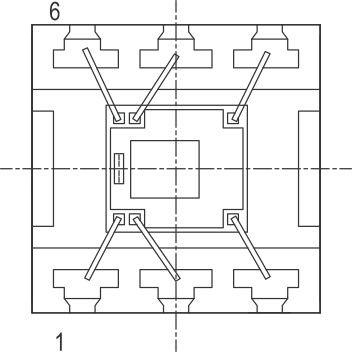
OPT3002 pin1_sbos681.gif Figure 25. Package Orientation Visual Reference of Pin 1
(Top View)
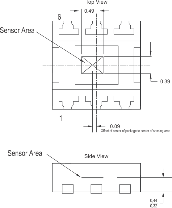
OPT3002 sensor_location_sbos681.gif Figure 26. Mechanical Outline Showing Sensing Area Location
(Top and Side Views)