SLES117B August 2004 – December 2015 PCM1794A
PRODUCTION DATA.
- 1 Features
- 2 Applications
- 3 Description
- 4 Revision History
- 5 Pin Configuration and Functions
- 6 Specifications
- 7 Detailed Description
- 8 Application and Implementation
- 9 Power Supply Recommendations
- 10Layout
- 11Device and Documentation Support
- 12Mechanical, Packaging, and Orderable Information
Package Options
Refer to the PDF data sheet for device specific package drawings
Mechanical Data (Package|Pins)
- DB|28
Thermal pad, mechanical data (Package|Pins)
Orderable Information
6 Specifications
6.1 Absolute Maximum Ratings
over operating free-air temperature range (unless otherwise noted) (1)| MIN | MAX | UNIT | ||
|---|---|---|---|---|
| Supply Voltage | VCC1, VCC2L, VCC2R | –0.3 | 6.5 | V |
| VDD | –0.3 | 4 | ||
| Supply voltage differences: VCC1, VCC2L, VCC2R | ±0.1 | V | ||
| Ground voltage differences: AGND1, AGND2, AGND3L, AGND3R, DGND | ±0.1 | V | ||
| Digital input voltage | LRCK, DATA, BCK, SCK, FMT1, FMT0, MONO, CHSL, DEM, MUTE, RST | –0.3 | 6.5 | V |
| ZERO | –0.3 | (VDD + 0.3 V) < 4 | ||
| Analog input voltage | –0.3 | (VCC + 0.3 V) < 6.5 | V | |
| Input current (any pins except supplies) | ±10 | mA | ||
| Ambient temperature under bias | –40 | 125 | °C | |
| Junction temperature | 150 | °C | ||
| Lead temperature (soldering, 5 s) | 260 | °C | ||
| Package temperature (IR reflow, peak) | 250 | °C | ||
| Storage temperature, Tstg | –55 | 150 | °C | |
(1) Stresses beyond those listed under Absolute Maximum Ratings may cause permanent damage to the device. These are stress ratings only, which do not imply functional operation of the device at these or any other conditions beyond those indicated under Recommended Operating Conditions. Exposure to absolute-maximum-rated conditions for extended periods may affect device reliability.
6.2 ESD Ratings
| VALUE | UNIT | |||
|---|---|---|---|---|
| V(ESD) | Electrostatic discharge | Human-body model (HBM), per ANSI/ESDA/JEDEC JS-001(1) | ±2500 | V |
| Charged-device model (CDM), per JEDEC specification JESD22-C101(2) | ±1500 | |||
(1) JEDEC document JEP155 states that 500-V HBM allows safe manufacturing with a standard ESD control process.
(2) JEDEC document JEP157 states that 250-V CDM allows safe manufacturing with a standard ESD control process.
6.3 Recommended Operating Conditions
over operating free-air temperature range (unless otherwise noted)| MIN | NOM | MAX | UNIT | |||
|---|---|---|---|---|---|---|
| Supply voltage | VDD | 3 | 3.3 | 3.6 | VDC | |
| VCC1 VCC2L VCC2R |
4.75 | 5 | 5.25 | VDC | ||
| TJ | Operation temperature | —25 | 85 | °C | ||
6.4 Thermal Information
| THERMAL METRIC(1) | PCM1794A | UNIT | |
|---|---|---|---|
| DB (SSOP) | |||
| 28 PINS | |||
| RθJA | Junction-to-ambient thermal resistance | 66.4 | °C/W |
| RθJC(top) | Junction-to-case (top) thermal resistance | 25.4 | °C/W |
| RθJB | Junction-to-board thermal resistance | 27.5 | °C/W |
| ψJT | Junction-to-top characterization parameter | 2.3 | °C/W |
| ψJB | Junction-to-board characterization parameter | 27.1 | °C/W |
| RθJC(bot) | Junction-to-case (bottom) thermal resistance | — | °C/W |
(1) For more information about traditional and new thermal metrics, see the Semiconductor and IC Package Thermal Metrics application report, SPRA953.
6.5 Electrical Characteristics
all specifications at TA = 25°C, VCC1 = VCC2L = VCC2R = 5 V, VDD = 3.3 V, fS = 44.1 kHz, system clock = 256 fS, and 24-bit data, unless otherwise noted| PARAMETER | TEST CONDITIONS | MIN | TYP | MAX | UNIT | ||
|---|---|---|---|---|---|---|---|
| DATA FORMAT | |||||||
| fS | Sampling frequency | 10 | 200 | kHz | |||
| System clock frequency | 128, 192, 256, 384, 512, 768 | fS | |||||
| DIGITAL INPUT/OUTPUT | |||||||
| Logic family | TTL compatible | ||||||
| VIH | Input logic level high | 2 | VDC | ||||
| VIL | Input logic level low | 0.8 | VDC | ||||
| IIH | Input logic current high | VIN = VDD | 10 | µA | |||
| IIL | Input logic current low | VIN = 0 V | –10 | µA | |||
| VOH | Output logic level high | IOH = –2 mA | 2.4 | VDC | |||
| VOL | Output logic level low | IOL = 2 mA | 0.4 | VDC | |||
| DYNAMIC PERFORMANCE (2-V RMS OUTPUT)(1)(2) | |||||||
| THD+N at VOUT = 0 dB | fS = 44.1 kHz | 0.0004% | 0.0008% | ||||
| fS = 96 kHz | 0.0008% | ||||||
| fS = 192 kHz | 0.0015% | ||||||
| Dynamic range | EIAJ, A-weighted, fS = 44.1 kHz | 123 | 127 | dB | |||
| EIAJ, A-weighted, fS = 96 kHz | 127 | ||||||
| EIAJ, A-weighted, fS = 192 kHz | 127 | ||||||
| Signal-to-noise ratio | EIAJ, A-weighted, fS = 44.1 kHz | 123 | 127 | dB | |||
| EIAJ, A-weighted, fS = 96 kHz | 127 | ||||||
| EIAJ, A-weighted, fS = 192 kHz | 127 | ||||||
| Channel separation | fS = 44.1 kHz | 120 | 123 | dB | |||
| fS = 96 kHz | 122 | ||||||
| fS = 192 kHz | 120 | ||||||
| Level linearity error | VOUT = –120 dB | ±1 | dB | ||||
| DYNAMIC PERFORMANCE (4.5-V RMS Output)(1)(3) | |||||||
| THD+N at VOUT = 0 dB | fS = 44.1 kHz | 0.0004% | |||||
| fS = 96 kHz | 0.0008% | ||||||
| fS = 192 kHz | 0.0015% | ||||||
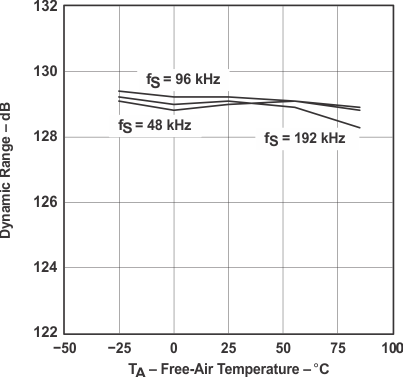
| Dynamic range | EIAJ, A-weighted, fS = 44.1 kHz | 129 | dB | ||||
| EIAJ, A-weighted, fS = 96 kHz | 129 | ||||||
| EIAJ, A-weighted, fS = 192 kHz | 129 | ||||||
| Signal-to-noise ratio | EIAJ, A-weighted, fS = 44.1 kHz | 129 | dB | ||||
| EIAJ, A-weighted, fS = 96 kHz | 129 | ||||||
| EIAJ, A-weighted, fS = 192 kHz | 129 | ||||||
| Channel separation | fS = 44.1 kHz | 124 | dB | ||||
| fS = 96 kHz | 123 | ||||||
| fS = 192 kHz | 121 | ||||||
| DYNAMIC PERFORMANCE (MONO MODE)(1)(3) | |||||||
| THD+N at VOUT = 0 dB | fS = 44.1 kHz | 0.0004% | |||||
| fS = 96 kHz | 0.0008% | ||||||
| fS = 192 kHz | 0.0015% | ||||||
| Dynamic range | EIAJ, A-weighted, fS = 44.1 kHz | 132 | dB | ||||
| EIAJ, A-weighted, fS = 96 kHz | 132 | ||||||
| EIAJ, A-weighted, fS = 192 kHz | 132 | ||||||
| Signal-to-noise ratio | EIAJ, A-weighted, fS = 44.1 kHz | 132 | dB | ||||
| EIAJ, A-weighted, fS = 96 kHz | 132 | ||||||
| EIAJ, A-weighted, fS = 192 kHz | 132 | ||||||
| ANALOG OUTPUT | |||||||
| Gain error | –6 | ±2 | 6 | % of FSR | |||
| Gain mismatch, channel-to-channel | –3 | ±0.5 | 3 | % of FSR | |||
| Bipolar zero error | At BPZ | –2 | ±0.5 | 2 | % of FSR | ||
| Output current | Full scale (0 dB) | 7.8 | mA p-p | ||||
| Center current | At BPZ | –6.2 | mA | ||||
| DIGITAL FILTER PERFORMANCE | |||||||
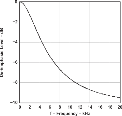
| De-emphasis error | ±0.004 | dB | |||||
| FILTER CHARACTERISTICS-1: SHARP ROLLOFF | |||||||
| Pass band | ±0.00001 dB | 0.454 fS | |||||
| –3 dB | 0.49 fS | ||||||
| Stop band | 0.546 fS | ||||||
| Pass-band ripple | ±0.00001 | dB | |||||
| Stop-band attenuation | Stop band = 0.546 fS | –130 | dB | ||||
| Delay time | 55/fS | s | |||||
| FILTER CHARACTERISTICS-2: SLOW ROLLOFF | |||||||
| Pass band | ±0.04 dB | 0.254 fS | |||||
| –3 dB | 0.46 fS | ||||||
| Stop band | 0.732 fS | ||||||
| Pass-band ripple | ±0.001 | dB | |||||
| Stop-band attenuation | Stop band = 0.732 fS | –100 | dB | ||||
| Delay time | 18 / fS | s | |||||
| POWER SUPPLY REQUIREMENTS | |||||||
| IDD | Digital supply current(4) | fS = 44.1 kHz | 12 | 15 | mA | ||
| fS = 96 kHz | 23 | ||||||
| fS = 192 kHz | 45 | ||||||
| ICC | Analog supply current(4) | fS = 44.1 kHz | 33 | 40 | mA | ||
| fS = 96 kHz | 35 | ||||||
| fS = 192 kHz | 37 | ||||||
| Power dissipation(4) | fS = 44.1 kHz | 205 | 250 | mW | |||
| fS = 96 kHz | 250 | ||||||
| fS = 192 kHz | 335 | ||||||
(1) Filter condition:
- THD+N: 20-Hz HPF, 20-kHz apogee LPF
- Dynamic range: 20-Hz HPF, 20-kHz AES17 LPF, A-weighted
- Signal-to-noise ratio: 20-Hz HPF, 20-kHz AES17 LPF, A-weighted
- Channel separation: 20-Hz HPF, 20-kHz AES17 LPF
- Analog performance specifications are measured using the System Two Cascade audio measurement system by Audio Precision™ in the averaging mode.
(2) Dynamic performance and dc accuracy are specified at the output of the postamplifier as shown in Figure 25.
(3) Dynamic performance and dc accuracy are specified at the output of the postamplifier as shown in Figure 26.
(4) Input is BPZ data.
6.6 Timing Requirements
| MIN | MAX | UNIT | ||
|---|---|---|---|---|
| SYSTEM CLOCK INPUT TIMING (see Figure 1) | ||||
| t(SCY) | System-clock pulse-cycle time | 13 | ns | |
| t(SCKH) | System-clock pulse duration, HIGH | 0.4 × t(SCY) | ns | |
| t(SCKL) | System-clock pulse duration, LOW | 0.4 × t(SCY) | ns | |
| EXTERNAL RESET TIMING (see Figure 2) | ||||
| t(RST) | Reset pulse duration, LOW | 20 | ns | |
| AUDIO INTERFACE TIMING (see Figure 3) | ||||
| t(BCY) | BCK pulse-cycle time | 70 | ns | |
| t(BCL) | BCK pulse duration, LOW | 30 | ns | |
| t(BCH) | BCK pulse duration, HIGH | 30 | ns | |
| t(BL) | BCK rising edge to LRCK edge | 10 | ns | |
| t(LB) | LRCK edge to BCK rising edge | 10 | ns | |
| t(DS) | DATA setup time | 10 | ns | |
| t(DH) | DATA hold time | 10 | ns | |
| LRCK clock duty | 50% ± 2-bit clocks | |||
 Figure 1. System Clock Input Timing
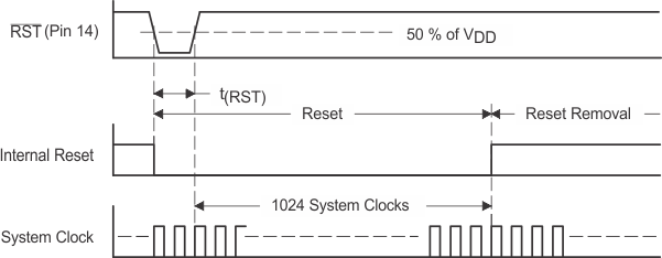 Figure 2. External Reset Timing
 Figure 3. Timing of Audio Interface
6.7 Typical Characteristics
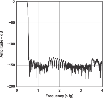
Frequency Response, Sharp Rolloff
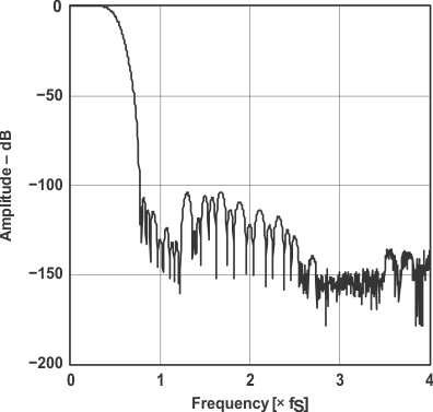
Frequency Response, Slow Rolloff
| fS = 44.1 kHz | ||
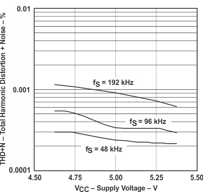
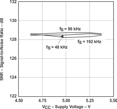
| TA = 25°C | VOUT = 4.5 VRMS | |
| VDD = 3.3 V | Measurement circuit is Figure 26 | |
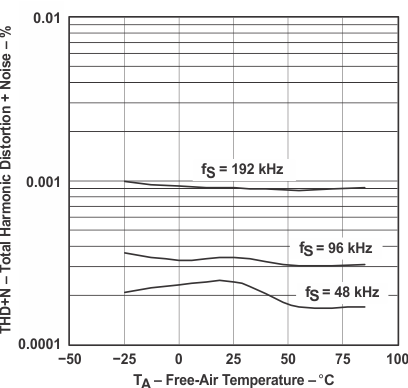
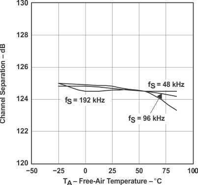
vs Free-Air Temperature
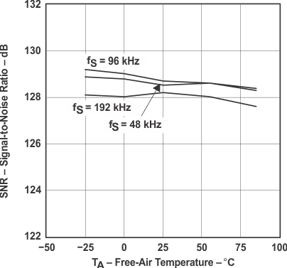
| VCC = 5 V | VOUT = 4.5 VRMS |
| VDD = 3.3 V | Measurement circuit is Figure 26. |
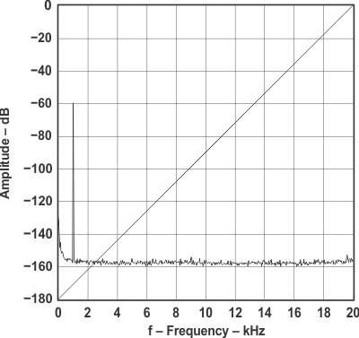
| VCC = 5 V | Measurement circuit is Figure 26 | |
| TA = 25°C | VDD = 3.3 V | fS = 48 kHz, 32768 point 8 average |
–60-db Output Spectrum, BW = 20 kHz
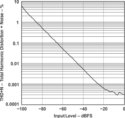
| VCC = 5 V | Measurement circuit is Figure 26 | |||
| VDD = 3.3 V | fS = 48 kHz, TA = 25°C | |||
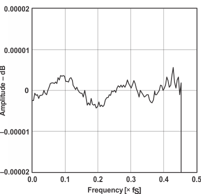
Pass-Band Ripple, Sharp Rolloff
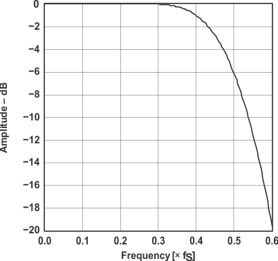
Transition Characteristics, Slow Rolloff
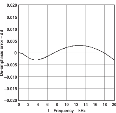
| fS = 44.1 kHz | ||
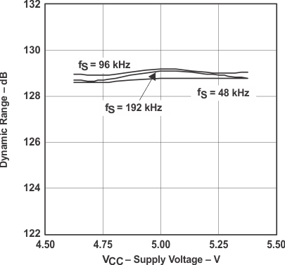
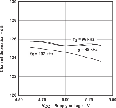
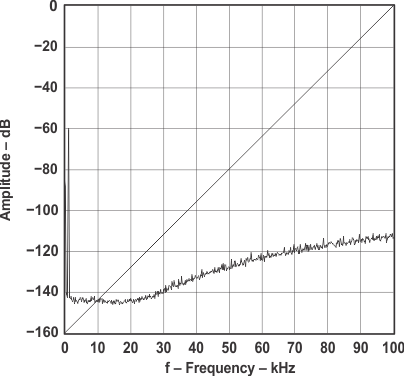
| VCC = 5 V | Measurement circuit is Figure 26 | |
| TA = 25°C | VDD = 3.3 V | fS = 48 kHz, 32768 point 8 average |
–60-db Output Spectrum, BW = 100 kHz