SLAS859C May 2012 – May 2015 PCM5100A , PCM5100A-Q1 , PCM5101A , PCM5101A-Q1 , PCM5102A , PCM5102A-Q1
PRODUCTION DATA.
- 1 Features
- 2 Applications
- 3 Description
- 4 Simplified System Diagram
- 5 Revision History
- 6 Device Comparison
- 7 Pin Configuration and Functions
- 8 Specifications
- 9 Detailed Description
- 10Applications and Implementation
- 11Power Supply Recommendations
- 12Layout
- 13Device and Documentation Support
- 14Mechanical, Packaging, and Orderable Information
Package Options
Mechanical Data (Package|Pins)
- PW|20
Thermal pad, mechanical data (Package|Pins)
- PW|20
Orderable Information
9 Detailed Description
9.1 Overview
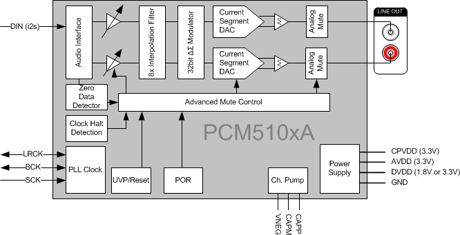
The integrated PLL on the device provided adds the flexibility to remove the system clock (commonly known as master clock), allowing a 3-wire I2S connection and reducing system EMI.
Powersense undervoltage protection utilizes a two-level mute system. Upon clock error or system power failure, the device digitally attenuates the data (or last known good data) and then mutes the analog circuit.
Compared with existing DAC technology, the PCM510xA devices offer up to 20 dB lower out-of-band noise, reducing EMI and aliasing in downstream amplifiers/ADCs. (from traditional 100-kHz OBN measurements to 3 MHz).
The PCM510xA devices accept industry-standard audio data formats with 16- to 32-bit data. Sample rates up to 384 kHz are supported.
9.3 Feature Description
9.3.1 Terminology
Sampling frequency is symbolized by fS. Full scale is symbolized by FS. Sample time as a unit is symbolized by tS.
9.3.2 Audio Data Interface
9.3.2.1 Audio Serial Interface
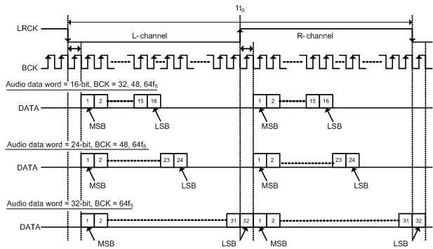
The audio interface port is a 3-wire serial port with the signals LRCK, BCK, and DIN. BCK is the serial audio bit clock, used to clock the serial data present on DIN into the serial shift register of the audio interface. Serial data is clocked into the PCM510xA on the rising edge of BCK. LRCK is the serial audio left/right word clock. LRCK polarity for left/right is given by the format selected.
Table 2. PCM510xA Audio Data Formats, Bit Depths and Clock Rates
| CONTROL MODE | FORMAT | DATA BITS | MAX LRCK FREQUENCY [fS] | SCK RATE [x fS] | BCK RATE [x fS] |
|---|---|---|---|---|---|
| Hardware Control | I2S/LJ | 32, 24, 20, 16 | Up to 192 kHz | 128 – 3072 (≤50MHz) | 64, 48, 32 |
| 384 kHz | 64, 128 | 64, 48, 32 |
The PCM510xA requires the synchronization of LRCK and system clock, but does not need a specific phase relation between LRCK and system clock.
If the relationship between LRCK and system clock changes more than ±5 SCK, internal operation (using an onchip oscillator) is initialized within one sample period and analog outputs are forced to the bipolar zero level until resynchronization between LRCK and system clock is completed.
If the relationship between LRCK and BCK are invalid more than 4 LRCK periods, internal operation (using an onchip oscillator) is initialized within one sample period and analog outputs are forced to the bipolar zero level until resynchronization between LRCK and BCK is completed.
9.3.2.2 PCM Audio Data Formats
The PCM510xA supports industry-standard audio data formats, including standard I2S and left-justified. Data formats are selected using the FMT (pin 16), Low for I2S, and High for Left-justified. All formats require binary twos-complement, MSB-first audio data; up to 32-bit audio data is accepted.
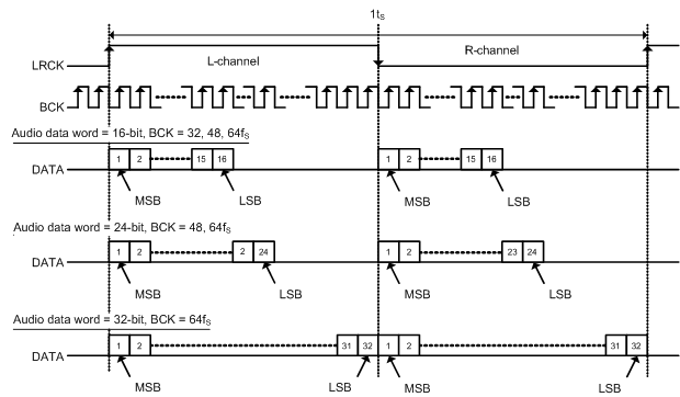 Figure 13. Left Justified Audio Data Format
9.3.2.3 Zero Data Detect
The PCM510xA has a zero-data detect function. When the device detects continuous zero data, it enters a full analog mute condition. The PCM510xA counts zero data over 1024 LRCKs (21ms @ 48kHz) before setting analog mute.
In Hardware mode, the device uses default values. By default, Both L-ch and R-ch have to be zero data for zero data detection to begin the muting process etc.
9.3.3 XSMT Pin (Soft Mute / Soft Un-Mute)
An external digital host controls the PCM510xA soft mute function by driving the XSMT pin with a specific minimum rise time (tr) and fall time (tf) for soft mute and soft un-mute. The PCM510xA requires tr and tf times of less than 20ns. In the majority of applications, this is no problem, however, traces with high capacitance may have issues.
When the XSMT pin is shifted from high to low (3.3 V to 0 V), a soft digital attenuation ramp begins. –1-dB attenuation is then applied every sample time from 0 dBFS to –∞. The soft attenuation ramp takes 104 samples.
When the XSMT pin is shifted from low to high (0 V to 3.3 V), a soft digital “un-mute” is started. 1-dB gain steps are applied every sample time from –∞ to 0 dBFS. The un-mute takes 104 samples.
In systems where XSMT is not required, it can be directly connected to AVDD.
9.3.4 Audio Processing
9.3.4.1 Interpolation Filter
The PCM510xA provides two types of interpolation filter. Users can select which filter to use by using the FLT pin (pin 11).
Table 3. Digital Interpolation Filter Options
| FLT Pin | Description |
| 0 | FIR normal x8/x4/x2/x1 interpolation filters |
| 1 | IIR low-latency x8/x4/x2/x1 interpolation filters |
The normal x8 / x4 / x2 / x1(bypass) interpolation filter is programmed for sample rates from 8 kHz to 384 kHz.
Table 4. Normal x8 Interpolation Filter
| Parameter | Condition | Value (Typ) | Value (Max) | Units |
| Filter gain pass band | 0 ……. 0.45fS | ±0.02 | dB | |
| Filter gain stop band | 0.55fS ….. 7.455fS | –60 | dB | |
| Filter group delay | 22tS | s |
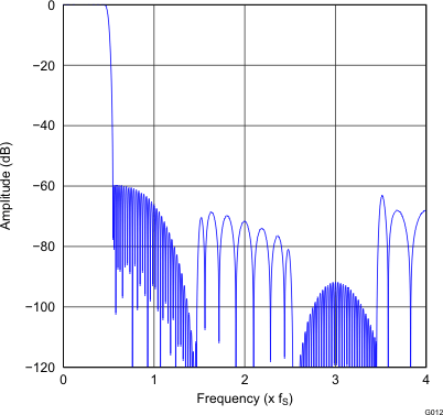 Figure 15. Normal x8 Interpolation Filter Frequency Response
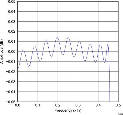 Figure 17. Normal x8 Interpolation Filter Passband Ripple
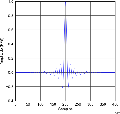 Figure 16. Normal x8 Interpolation Filter Impulse Response
The normal x4 / x2 / x1 (bypass) interpolation filter is programmed for sample rates from 8 kHz to 384 kHz.
Table 5. Normal x4 Interpolation Filter
| Parameter | Condition | Value (Typ) | Value (Max) | Units |
| Filter gain pass band | 0 ……. 0.45fS | ±0.02 | dB | |
| Filter gain stop band | 0.55fS ….. 7.455fS | –60 | dB | |
| Filter group delay | 22tS | s |
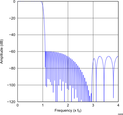 Figure 18. Normal x4 Interpolation Filter Frequency Response
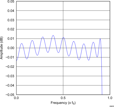 Figure 20. Normal x4 Interpolation Filter Passband Ripple
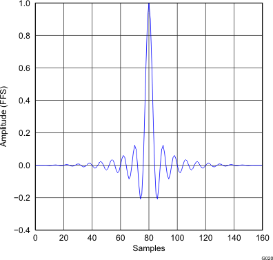 Figure 19. Normal x4 Interpolation Filter Impulse Response
Table 6. Normal x2 Interpolation Filter
| Parameter | Condition | Value (Typ) | Value (Max) | Units |
| Filter gain pass band | 0 ……. 0.45fS | ±0.02 | dB | |
| Filter gain stop band | 0.55fS ….. 7.455fS | –60 | dB | |
| Filter group delay | 22tS | s |
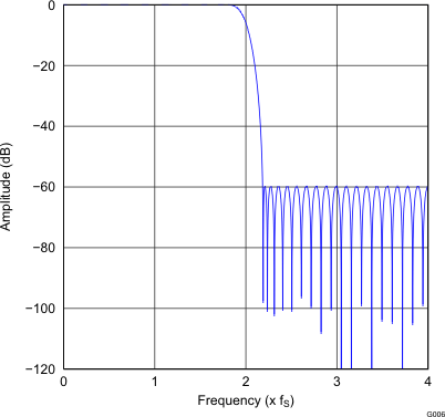 Figure 21. Normal x2 Interpolation Filter Frequency Response
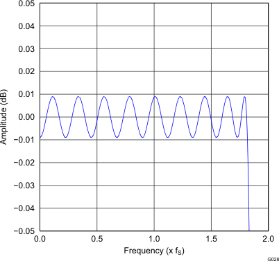 Figure 23. Normal x2 Interpolation Filter Passband Ripple
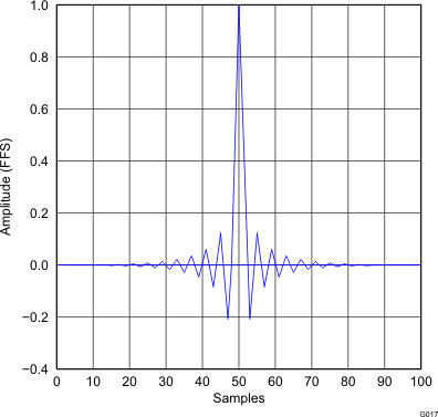 Figure 22. Normal x2 Interpolation Filter Impulse Response
The low-latency x8 / x4 / x2 / x1 (bypass) interpolation filter is programmed for sample rates from 8 kHz to 384 kHz.
Table 7. Low Latency x8 Interpolation Filter
| Parameter | Condition | Value (Typ) | Units |
| Filter gain pass band | 0 ……. 0.45fS | ±0.0001 | dB |
| Filter gain stop band | 0.55fS ….. 7.455fS | –52 | dB |
| Filter group delay | 3.5tS | s |
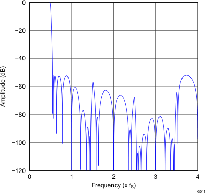 Figure 24. Low Latency x8 Interpolation Filter Frequency Response
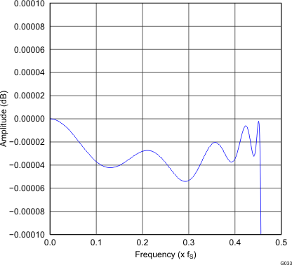 Figure 26. Low Latency x8 Interpolation Filter Passband Ripple
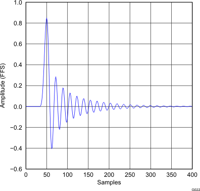 Figure 25. Low Latency x8 Interpolation Filter Impulse Response
Table 8. Low Latency x4 Interpolation Filter
| Parameter | Condition | Value (Typ) | Units |
| Filter gain pass band | 0 ……. 0.45fS | ±0.0001 | dB |
| Filter gain stop band | 0.55fS ….. 3.455fS | –52 | dB |
| Filter group delay | 3.5tS | s |
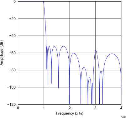 Figure 27. Low Latency x4 Interpolation Filter Frequency Response
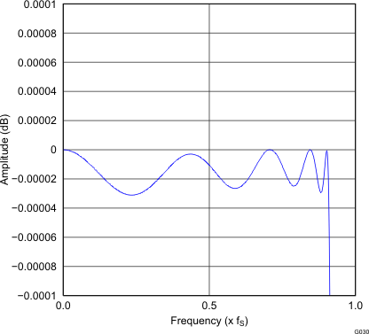 Figure 29. Low Latency x4 Interpolation Filter Passband Ripple
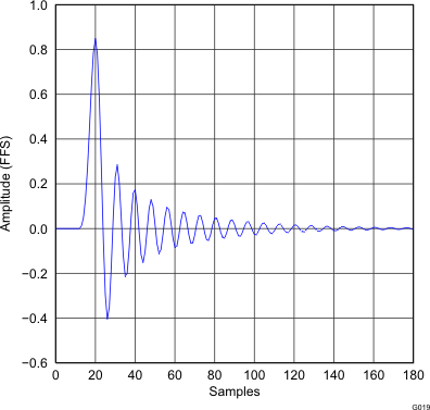 Figure 28. Low Latency x4 Interpolation Filter Impulse Response
Table 9. Low Latency x2 Interpolation Filter
| Parameter | Condition | Value (Typ) | Units |
| Filter gain pass band | 0 ……. 0.45fS | ±0.0001 | dB |
| Filter gain stop band | 0.55fS ….. 1.455fS | –52 | dB |
| Filter group delay | 3.5tS | s |
space
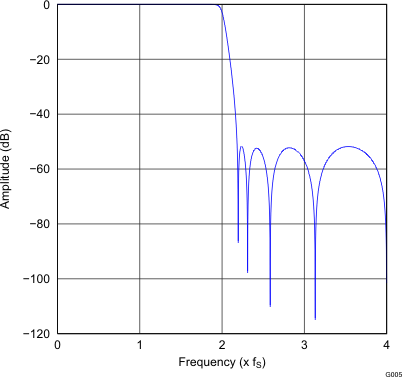 Figure 30. Low Latency x2 Interpolation Filter Frequency Response
 Figure 32. Low Latency x2 Interpolation Filter Passband Ripple
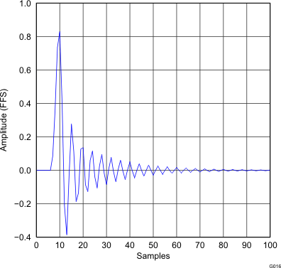 Figure 31. Low Latency x2 Interpolation Filter Impulse Response
9.3.5 Reset and System Clock Functions
9.3.5.1 Clocking Overview
The PCM510xA devices have flexible systems for clocking. Internally, the device requires a number of clocks, mostly at related clock rates to function correctly. All of these clocks can be derived from the serial audio interface in one form or another.
The data flows at the sample rate (fS). Once the data is brought into the serial audio interface, it gets processed, interpolated and modulated all the way to 128 × fS before arriving at the current segments for the final digital to analog conversion.
The serial audio interface typically has 4 connections SCK (system master clock), BCK (bit clock), LRCK (left right word clock) and DIN (data). The device has an internal PLL that is used to take either SCK or BCK and create the higher rate clocks required by the interpolating processor and the DAC clock. This allows the device to operate with or without an external SCK.
9.3.5.2 Clock Slave Mode With Master/System Clock (SCK) Input (4 Wire I2S)
The PCM510xA requires a system clock to operate the digital interpolation filters and advanced segment DAC modulators. The system clock is applied at the SCK input and supports up to 50 MHz. The PCM510xA system-clock detection circuit automatically senses the system-clock frequency. Common audio sampling frequencies in the bands of 8 kHz, 16 kHz, (32 kHz - 44.1 kHz - 48 kHz), (88.2kHz - 96kHz), (176.4 kHz - 192 kHz), and 384 kHz with ±4% tolerance are supported. Values in the parentheses are grouped when detected, e.g. 88.2kHZ and 96kHz are detected as "double rate," 32kHz, 44.1kHz and 48kHz will be detected as "single rate".
The sampling frequency detector sets the clock for the digital filter, Delta Sigma Modulator (DSM) and the Negative Charge Pump (NCP) automatically. Table 10 shows examples of system clock frequencies for common audio sampling rates.
SCK rates that are not common to standard audio clocks, between 1 MHz and 50 MHz, are only supported in software mode, available only in the PCM512x, PCM514x, and PCM5242 devices, by configuring various PLL and clock-divider registers. This programmability allows the device to become a clock master and drive the host serial port with LRCK and BCK, from a non-audio related clock (for example, using 12 MHz to generate 44.1 kHz [LRCK] and 2.8224 MHz [BCK]).
Table 10. System Master Clock Inputs for Audio Related Clocks
| Sampling Frequency | System Clock Frequency (fSCK) (MHz) | |||||||||||
| 64 fS | 128 fS | 192 fS | 256 fS | 384 fS | 512 fS | 768 fS | 1024 fS | 1152 fS | 1536 fS | 2048 fS | 3072 fS | |
| 8 kHz | –(1) | 1.024(2) | 1.536(2) | 2.048 | 3.072 | 4.096 | 6.144 | 8.192 | 9.216 | 12.288 | 16.384 | 24.576 |
| 16 kHz | –(1) | 2.048(2) | 3.072(2) | 4.096 | 6.144 | 8.192 | 12.288 | 16.384 | 18.432 | 24.576 | 36.864 | 49.152 |
| 32 kHz | –(1) | 4.096(2) | 6.144(2) | 8.192 | 12.288 | 16.384 | 24.576 | 32.768 | 36.864 | 49.152 | –(1) | –(1) |
| 44.1 kHz | –(1) | 5.6488(2) | 8.4672(2) | 11.2896 | 16.9344 | 22.5792 | 33.8688 | 45.1584 | –(1) | –(1) | –(1) | –(1) |
| 48 kHz | –(1) | 6.144(2) | 9.216(2) | 12.288 | 18.432 | 24.576 | 36.864 | 49.152 | –(1) | –(1) | –(1) | –(1) |
| 88.2 kHz | –(1) | 11.2896(2) | 16.9344 | 22.5792 | 33.8688 | 45.1584 | –(1) | –(1) | –(1) | –(1) | –(1) | –(1) |
| 96 kHz | –(1) | 12.288(2) | 18.432 | 24.576 | 36.864 | 49.152 | –(1) | –(1) | –(1) | –(1) | –(1) | –(1) |
| 176.4 kHz | –(1) | 22.579 | 33.8688 | 45.1584 | –(1) | –(1) | –(1) | –(1) | –(1) | –(1) | –(1) | –(1) |
| 192 kHz | –(1) | 24.576 | 36.864 | 49.152 | –(1) | –(1) | –(1) | –(1) | –(1) | –(1) | –(1) | –(1) |
| 384 kHz | 24.576 | 49.152 | –(1) | –(1) | –(1) | –(1) | –(1) | –(1) | –(1) | –(1) | –(1) | –(1) |
9.3.5.3 Clock Slave Mode with BCK PLL to Generate Internal Clocks (3-Wire PCM)
The system clock PLL mode allows designers to use a simple 3-wire I2S audio source. The 3-wire source reduces the need for a high frequency SCK, making PCB layout easier, and reduces high frequency electromagnetic interference.
The internal PLL is disabled as soon as an external SCK is supplied.
The device starts up expecting an external SCK input, but if BCK and LRCK start correctly while SCK remains at ground level for 16 successive LRCK periods, then the internal PLL starts, automatically generating an internal SCK from the BCK reference. Specific BCK rates are required to generate an appropriate master clock.Table 11 describes the minimum and maximum BCK per LRCK for the integrated PLL to automatically generate an internal SCK.
Table 11. BCK Rates (MHz) by LRCK Sample Rate for PCM510xA PLL Operation
| BCK (fS) | ||
| Sample f (kHz) | 32 | 64 |
| 8 | – | – |
| 16 | – | 1.024 |
| 32 | 1.024 | 2.048 |
| 44.1 | 1.4112 | 2.8224 |
| 48 | 1.536 | 3.072 |
| 96 | 3.072 | 6.144 |
| 192 | 6.144 | 12.288 |
| 384 | 12.288 | 24.576 |
9.4 Device Functional Modes
9.4.1 External SCK and PLL Activation
As discussed in Clock Slave Mode with BCK PLL to Generate Internal Clocks (3-Wire PCM), the internal PLL of a PCM510xA device supplies a SCK if an external SCK is not present at powerup.
9.4.1.1 Interpolation Filter Modes
Interpolation-filter options are controlled by the FLT pin. See Table 3.
9.4.1.2 44.1kHz De-emphasis
De-emphasis control for 44.1-kHz fS is controlled by the DEMP pin. See Pin Configuration and Functions.
9.4.1.3 Audio Format
Audio format is selected by the FMT pin. See Pin Configuration and Functions.
