SLAS859C May 2012 – May 2015 PCM5100A , PCM5100A-Q1 , PCM5101A , PCM5101A-Q1 , PCM5102A , PCM5102A-Q1
PRODUCTION DATA.
- 1 Features
- 2 Applications
- 3 Description
- 4 Simplified System Diagram
- 5 Revision History
- 6 Device Comparison
- 7 Pin Configuration and Functions
- 8 Specifications
- 9 Detailed Description
- 10Applications and Implementation
- 11Power Supply Recommendations
- 12Layout
- 13Device and Documentation Support
- 14Mechanical, Packaging, and Orderable Information
Package Options
Mechanical Data (Package|Pins)
- PW|20
Thermal pad, mechanical data (Package|Pins)
- PW|20
Orderable Information
8 Specifications
8.1 Absolute Maximum Ratings
over operating free-air temperature range (unless otherwise noted)| MIN | MAX | UNIT | ||
|---|---|---|---|---|
| Supply voltage | AVDD, CPVDD, DVDD | –0.3 | 3.9 | V |
| LDO with DVDD at 1.8 V | –0.3 | 2.25 | ||
| Digital input voltage | DVDD at 1.8 V | –0.3 | 2.25 | |
| DVDD at 3.3 V | –0.3 | 3.9 | ||
| Analog input voltage | –0.3 | 3.9 | ||
| Operating junction temperature range | –40 | 130 | °C | |
| Storage temperature, Tstg | –65 | 150 | °C | |
8.2 ESD Ratings
| VALUE | UNIT | |||
|---|---|---|---|---|
| V(ESD) | Electrostatic discharge | Human-body model (HBM), per ANSI/ESDA/JEDEC JS-001(1) | ±2000 | V |
| Charged-device model (CDM), per JEDEC specification JESD22-C101(2) | ±750 | |||
(1) JEDEC document JEP155 states that 500-V HBM allows safe manufacturing with a standard ESD control process.
(2) JEDEC document JEP157 states that 250-V CDM allows safe manufacturing with a standard ESD control process.
8.3 Recommended Operating Conditions
| MIN | NOM | MAX | UNIT | ||||
|---|---|---|---|---|---|---|---|
| AVDD | Analog power supply voltage range | Referenced to AGND(1) | VCOM mode | 3 | 3.3 | 3.46 | V |
| VREF mode | 3.2 | 3.3 | 3.46 | ||||
| DVDD | Digital power supply voltage range | Referenced to DGND(1) | 1.8 V DVDD | 1.65 | 1.8 | 1.95 | V |
| 3.3 V DVDD | 3.1 | 3.3 | 3.46 | ||||
| CPVDD | Charge pump supply voltage range | Referenced to CPGND(1) | 3.1 | 3.3 | 3.46 | V | |
| MCLK | Master clock frequency | 50 | MHz | ||||
| LOL, LOR | Stereo line output load resistance | 1 | 10 | kΩ | |||
| CLOUT | Digital output load capacitance | 10 | pF | ||||
| TJ | Operating junction temperature range | –40 | 130 | °C | |||
(1) All grounds on board are tied together; they must not differ in voltage by more than 0.2 V max, for any combination of ground signals.
8.4 Thermal Information
| THERMAL METRIC(1) | PW | UNIT | |
|---|---|---|---|
| 20 PINS | |||
| RθJA | Junction-to-ambient thermal resistance | 91.2 | °C/W |
| RθJC(top) | Junction-to-case (top) thermal resistance | 25.3 | |
| RθJB | Junction-to-board thermal resistance | 42 | |
| ψJT | Junction-to-top characterization parameter | 1 | |
| ψJB | Junction-to-board characterization parameter | 41.5 | |
| RθJC(bot) | Junction-to-case (bottom) thermal resistance | — | |
(1) For more information about traditional and new thermal metrics, see the IC Package Thermal Metrics application report, SPRA953.
8.5 Electrical Characteristics
Q1 Automotive grade devices are specified for TA = –40°C to 125°C. Consumer grade (non-Q1) devices are specified at TA = 25°C. All devices in the family are characterized with AVDD = CPVDD = DVD = 3.3 V, fS = 48 kHz, system clock = 512 fS and 24-bit data unless otherwise noted.| PARAMETER | TEST CONDITIONS | MIN | TYP | MAX | UNIT | ||
|---|---|---|---|---|---|---|---|
| Resolution | 16 | 24 | 32 | Bits | |||
| Data Format (PCM Mode) | |||||||
| Audio data bit length | 16 | 24 | 32 | Bits | |||
| fS(7) | Sampling frequency | 8 | 384 | kHz | |||
| fSCK | System clock frequency | Clock multiples: 64, 128, 192, 256, 384, 512, 768, 1024, 1152, 1536, 2048, or 3072 | 50 | MHz | |||
| Digital Input/Output for non-Q1 Consumer Grade Devices | |||||||
| Logic family: 3.3 V LVCMOS compatible | |||||||
| VIH | Input logic level | 0.7×DVDD | V | ||||
| VIL | 0.3×DVDD | ||||||
| IIH | Input logic current | VIN = VDD | 10 | µA | |||
| IIL | VIN = 0 V | –10 | |||||
| VOH | Output logic level | IOH = –4 mA | 0.8×DVDD | V | |||
| VOL | IOL = 4 mA | 0.22×DVDD | |||||
| Logic family 1.8 V LVCMOS compatible | |||||||
| VIH | Input logic level | 0.7×DVDD | V | ||||
| VIL | 0.3×DVDD | ||||||
| IIH | Input logic current | VIN = VDD | 10 | µA | |||
| IIL | VIN = 0 V | –10 | |||||
| VOH | Output logic level | IOH = –2 mA | 0.8×DVDD | V | |||
| VOL | IOL = 2 mA | 0.22×DVDD | |||||
| Digital Input/Output for Q1 Automotive Grade Devices | |||||||
| Logic family: 3.3 V LVCMOS compatible | |||||||
| VIH | Input logic level | 0.7×DVDD | V | ||||
| VIL | 0.3×DVDD | ||||||
| IIH | Input logic current | VIN = VDD | 10 | µA | |||
| IIL | VIN = 0 V | –10 | |||||
| VOH | Output logic level | IOH = –4 mA | 0.8×DVDD | V | |||
| VOL | IOL = 4 mA | 0.22×DVDD | |||||
| Logic family 1.8 V LVCMOS compatible | |||||||
| VIH | Input logic level | 0.7×DVDD | V | ||||
| VIL | 0.3×DVDD | ||||||
| IIH | Input logic current | VIN = VDD | 10 | µA | |||
| IIL | VIN = 0 V | –10 | |||||
| VOH | Output logic level | IOH = –2 mA | 0.8×DVDD | V | |||
| VOL | IOL = 2 mA | 0.3×DVDD | |||||
| Dynamic Performance (PCM Mode)(1)(2) | |||||||
| THD+N at –1 dBFS(2) | fS = 48 kHz | PCM5102A | –93 | –83 | dB | ||
| PCM5101A | –92 | –82 | |||||
| PCM5100A | –90 | –80 | |||||
| fS = 96 kHz and 192 kHz | PCM5102A | –93 | |||||
| PCM5101A | –92 | ||||||
| PCM5100A | –90 | ||||||
| Dynamic range(2) | EIAJ, A-weighted, fS = 48 kHz | PCM5102A | 106 | 112 | |||
| PCM5101A | 100 | 106 | |||||
| PCM5100A | 95 | 100 | |||||
| EIAJ, A-weighted, fS = 96 kHz and 192 kHz | PCM5102A | 112 | |||||
| PCM5101A | 106 | ||||||
| PCM5100A | 100 | ||||||
| Signal-to-noise ratio(2) | EIAJ, A-weighted, fS = 48 kHz | PCM5102A | 112 | ||||
| PCM5101A | 106 | ||||||
| PCM5100A | 100 | ||||||
| EIAJ, A-weighted, fS = 96 kHz and 192 kHz | PCM5102A | 112 | |||||
| PCM5101A | 106 | ||||||
| PCM5100A | 100 | ||||||
| Signal to noise ratio with analog mute(2)(3) | EIAJ, A-weighted, fS = 48 kHz | 113 | 123 | ||||
| EIAJ, A-weighted, fS = 96 kHz and 192 kHz | 123 | ||||||
| Channel separation | fS = 48 kHz | PCM5102A | 100 | 109 | |||
| PCM5101A | 95 | 103 | |||||
| PCM5100A | 90 | 97 | |||||
| fS = 96 kHz | PCM5102A | 109 | |||||
| PCM5101A | 103 | ||||||
| PCM5100A | 97 | ||||||
| fS = 192 kHz | PCM5102A | 109 | |||||
| PCM5101A | 103 | ||||||
| PCM5100A | 97 | ||||||
| Analog Output | |||||||
| Output voltage | 2.1 | VRMS | |||||
| Gain error | –6 | ±2 | 6 | % of FSR | |||
| Gain error on Q1 Automotive Grade Devices | –7 | ±2 | 7 | % of FSR | |||
| Gain mismatch, channel-to-channel | –6 | ±2 | 6 | % of FSR | |||
| Gain mismatch, channel-to-channel on Q1 Devices | –6 | ±2 | 6 | % of FSR | |||
| PCM5100/1 bipolar zero error | At bipolar zero | –5 | ±1 | 5 | mV | ||
| PCM5102 Bipolar zero error | At bipolar zero | –2 | ±1 | 2 | mV | ||
| Load impedance | 1 | kΩ | |||||
| Filter Characteristics–1: Normal | |||||||
| Pass band | 0.45fS | ||||||
| Stop band | 0.55fS | ||||||
| Stop band attenuation | –60 | dB | |||||
| Pass-band ripple | ±0.02 | ||||||
| Delay time | 20tS | s | |||||
| Filter Characteristics–2: Low Latency | |||||||
| Pass band | 0.47fS | ||||||
| Stop band | 0.55fS | ||||||
| Stop band attenuation | –52 | dB | |||||
| Pass-band ripple | ±0.0001 | ||||||
| Delay time | 3.5tS | s | |||||
| Power Supply Requirements | |||||||
| DVDD | Digital supply voltage | Target DVDD = 1.8 V | 1.65 | 1.8 | 1.95 | VDC | |
| DVDD | Digital supply voltage | Target DVDD = 3.3 V | 3 | 3.3 | 3.6 | VDC | |
| AVDD | Analog supply voltage | 3 | 3.3 | 3.6 | |||
| CPVDD | Charge-pump supply voltage | 3 | 3.3 | 3.6 | |||
| IDD | DVDD supply current at 1.8 V(4) | fS = 48 kHz | 7 | mA | |||
| fS = 96 kHz | 8 | ||||||
| fS = 192 kHz | 9 | ||||||
| IDD | DVDD supply current at 1.8 V(5) | fS = 48 kHz | 7 | mA | |||
| fS = 96 kHz | 8 | ||||||
| fS = 192 kHz | 9 | ||||||
| IDD | DVDD supply current at 1.8 V(6) | Standby | 0.3 | mA | |||
| IDD | DVDD supply current at 3.3 V(4) | fS = 48 kHz | 7 | 12 | mA | ||
| fS = 96 kHz | 8 | ||||||
| fS = 192 kHz | 9 | ||||||
| IDD | DVDD supply current at 3.3 V(5) | fS = 48 kHz | 8 | 13 | mA | ||
| fS = 96 kHz | 9 | ||||||
| fS = 192 kHz | 10 | ||||||
| IDD | DVDD supply current at 3.3 V(6) | Standby | 0.5 | 0.8 | mA | ||
| IDD | AVDD / CPVDD supply current(4) | fS = 48 kHz | 11 | 16 | mA | ||
| fS = 96 kHz | 11 | ||||||
| fS = 192 kHz | 11 | ||||||
| IDD | AVDD / CPVDD supply current(5) | fS = 48 kHz | 22 | 32 | mA | ||
| fS = 96 kHz | 22 | ||||||
| fS = 192 kHz | 22 | ||||||
| IDD | AVDD / CPVDD supply current(6) | fS = n/a | 0.2 | 0.4 | mA | ||
| Power dissipation, DVDD = 1.8 V(4) | fS = 48 kHz | 49 | 185 | mW | |||
| fS = 96 kHz | 51 | ||||||
| fS = 192 kHz | 53 | ||||||
| Power dissipation, DVDD = 1.8 V(5) | fS = 48 kHz | 85 | 187 | mW | |||
| fS = 96 kHz | 87 | ||||||
| fS = 192 kHz | 89 | ||||||
| Power dissipation, DVDD = 1.8 V(6) | fS = n/a (Power Down Mode) | 1 | mW | ||||
| Power dissipation, DVDD = 3.3 V(4) | fS = 48 kHz | 60 | 92.4 | mW | |||
| fS = 96 kHz | 63 | ||||||
| fS = 192 kHz | 66 | ||||||
| Power dissipation, DVDD = 3.3 V(5) | fS = 48 kHz | 99 | 148.5 | mW | |||
| fS = 96 kHz | 102 | ||||||
| fS = 192 kHz | 106 | ||||||
| Power dissipation, DVDD = 3.3 V(6) | fS = n/a (Power Down Mode) | 2 | 4 | mW | |||
(1) Filter condition: THD+N: 20-Hz HPF, 20-kHz AES17 LPF; Dynamic range: 20-Hz HPF, 20-kHz AES17 LPF; A-weighted signal-to-noise ratio: 20-Hz HPF, 20-kHz AES17 LPF; A-weighted channel separation: 20-Hz HPF, 20-kHz AES17 LPF. Analog performance specifications are measured using the System Two Cascade™ audio measurement system by Audio Precision™ in the RMS mode.
(2) Output load is 10 kΩ, with 470-Ω output resistor and a 2.2-nF shunt capacitor (see recommended output filter).
(3) Assert XSMT or both L-ch and R-ch PCM data are Bipolar Zero.
(4) Input is Bipolar Zero data.
(5) Input is 1 kHz –1 dBFS data.
(6) Power Down Mode
(7) One sample time is defined as the reciprocal of the sampling frequency. 1tS = 1/fS
8.6 Timing Requirements
Figure 1 shows the timing requirements for the system clock input. For optimal performance, use a clock source with low phase jitter and noise.| MIN | TYP | MAX | UNIT | |||
|---|---|---|---|---|---|---|
| tSCY | System clock pulse cycle time | 20 | 1000 | ns | ||
| tSCKH | System clock pulse width, High | DVDD = 1.8 V | 8 | ns | ||
| DVDD = 3.3 V | 9 | |||||
| tSCKL | System clock pulse width, Low | DVDD = 1.8 V | 8 | ns | ||
| DVDD = 3.3 V | 9 | |||||
 Figure 1. Timing Requirements for SCK Input
8.7 Timing Requirements, XSMT
| MIN | TYP | MAX | UNIT | ||
|---|---|---|---|---|---|
| tr | Rise time | 20 | ns | ||
| tf | Fall time | 20 | ns | ||
 Figure 2. XSMT Timing for Soft Mute and Soft Un-Mute
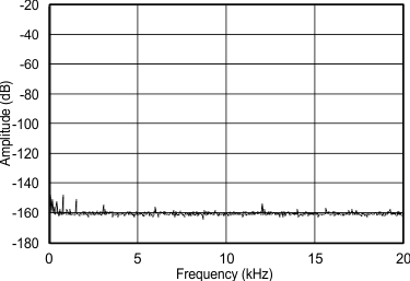
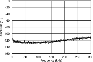
8.8 Typical Characteristics
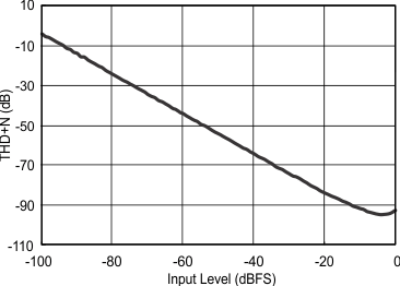
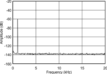
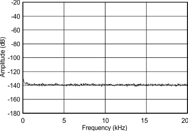
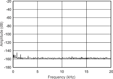
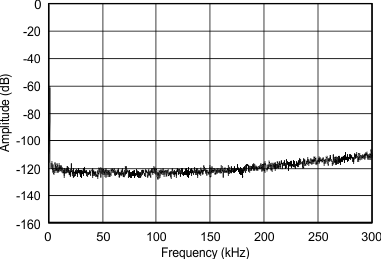
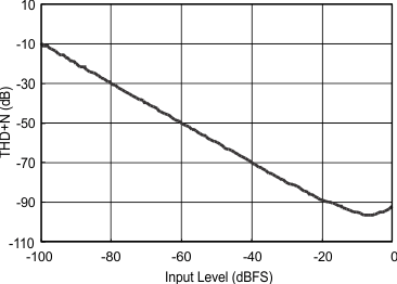
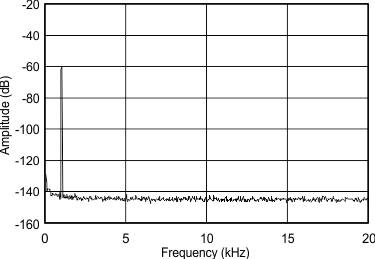
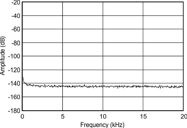
Q1 Automotive grade devices are specified for TA = –40°C to 125°C. Consumer grade (non-Q1) devices are specified at TA = 25°C, AVDD = CPVDD = DVDD = 3.3 V, fS = 48 kHz, system clock = 512 fS and 24-bit data unless otherwise noted.