SLDS185D March 2012 – June 2016 PGA450-Q1
PRODUCTION DATA.
- 1 Features
- 2 Applications
- 3 Description
- 4 Revision History
- 5 Pin Configuration and Functions
-
6 Specifications
- 6.1 Absolute Maximum Ratings
- 6.2 ESD Ratings: AEC Q100
- 6.3 ESD Ratings: IEC61000-4-2
- 6.4 Recommended Operating Conditions
- 6.5 Thermal Information
- 6.6 Electrical Characteristics
- 6.7 Electrical Characteristics — LIN 2.1 Slave and Buffered SCI
- 6.8 Electrical Characteristics — SPI Interface
- 6.9 Timing Requirements
- 6.10 Timing Requirements — LIN 2.1 Slave and Buffered SCI
- 6.11 Timing Requirements — SPI Interface
- 6.12 Switching Characteristics
- 6.13 Digital Datapath Filter Switching Characteristics
- 6.14 Typical Characteristics
-
7 Detailed Description
- 7.1 Overview
- 7.2 Functional Block Diagram
- 7.3
Feature Description
- 7.3.1 Power Supply Block
- 7.3.2 VREG
- 7.3.3 Clock
- 7.3.4 Low-Side Drive FETs
- 7.3.5 Burst Generator
- 7.3.6 Low-Noise Amplifier
- 7.3.7 Analog-to-Digital Converter
- 7.3.8 Digital Data Path
- 7.3.9 Transducer Saturation Time
- 7.3.10 Temperature Sensor
- 7.3.11 Free-Running Timer
- 7.3.12 GPIOs
- 7.3.13 8051W UART
- 7.3.14 8051 WARP Core
- 7.3.15 Memory
- 7.3.16
LIN 2.1 Slave and Buffered SCI
- 7.3.16.1 Physical Layer
- 7.3.16.2 LIN Slave Mode
- 7.3.16.3 SCI Buffered Mode
- 7.3.16.4 Connection of LIN Pin to 8051W
- 7.4 Device Functional Modes
- 7.5
Programming
- 7.5.1 SPI Interface
- 7.5.2 Diagnostics
- 7.5.3 8051W Interrupts
- 7.5.4 Instructions
- 7.5.5 8051W Port Usage
- 7.6
Register Maps
- 7.6.1
SFR Registers
- 7.6.1.1 I/O Ports (P0, P1, P2, P3) Registers
- 7.6.1.2 Stack Pointer Register (offset = 0x81) [reset = 0]
- 7.6.1.3 Data Pointer Registers
- 7.6.1.4 Power Control Register (offset = 0x87) [reset = 0]
- 7.6.1.5 Timer and Counter Control Register (offset = 0x88) [reset = 0]
- 7.6.1.6 Timer and Counter Mode Register (offset = 0x89) [reset = 0]
- 7.6.1.7 Timer and Counter Data Registers (TL0, TL1, TH0, TH1)
- 7.6.1.8 UART Control Register (offset = 0x98) [reset = 0]
- 7.6.1.9 UART Data Register (offset = 0x99) [reset = 0]
- 7.6.1.10 Interrupt Enable Register 0 (offset = 0xA8) [reset = 0]
- 7.6.1.11 Interrupt Enable Register 1 (offset = 0xE8) [reset = 0]
- 7.6.1.12 Interrupt Priority Register 0 (offset = 0xB8) [reset = 0]
- 7.6.1.13 Interrupt Priority Register 1 (offset = 0xF8) [reset = 0]
- 7.6.1.14 Program Status Word Register (offset = 0xD0) [reset = 0]
- 7.6.1.15 Accumulator Register (offset = 0xE0) [reset = 0]
- 7.6.1.16 B Register (offset = 0xF0) [reset = 0]
- 7.6.2
ESFR Registers
- 7.6.2.1 Bandpass Filter Coefficient B1 (BPF_B1) Register
- 7.6.2.2 Bandpass Filter Coefficient A2 (BPF_A2) Registers
- 7.6.2.3 Band-Pass Filter Coefficient A3 (BPF_A3) Register
- 7.6.2.4 Low-Pass Filter Coefficient B1 (LPF_B1) Registers
- 7.6.2.5 Low-Pass Filter Coefficient A2 (LPF_A2) Registers
- 7.6.2.6 Downsample Register (offset = 0xA5) [reset = 0]
- 7.6.2.7 BURST ON A Duration (ON_A) Registers
- 7.6.2.8 BURST OFFA Duration (OFF_A) Register
- 7.6.2.9 BURST ON B Duration (ON_B) Registers
- 7.6.2.10 BURST OFF B Duration (OFF_B) Register
- 7.6.2.11 Pulse Count A Register (offset = 0xAF) [reset = 0]
- 7.6.2.12 Pulse Count B Register (offset = 0xB1) [reset = 0]
- 7.6.2.13 Deadtime Register (offset = 0xB2) [reset = 0]
- 7.6.2.14 Burst Mode Register (offset = 0xB3) [reset = 0]
- 7.6.2.15 Temperature Sensor Register (offset = 0xB4) [reset = 0]
- 7.6.2.16 Saturation Deglitch Time Register (offset = 0xB5) [reset = 0]
- 7.6.2.17 Saturation Time Capture Register (offset = 0xB6) [reset = 0]
- 7.6.2.18 Control 1 Register (offset = 0xB7) [reset = 0]
- 7.6.2.19 Blanking Timer Register (offset = 0xB9) [reset = 0]
- 7.6.2.20 Free Running Timer (FRT) Registers
- 7.6.2.21 GPIO Control Register (offset = 0xBC) [reset = 0]
- 7.6.2.22 Clock Select Register (offset = 0xBD) [reset = 0]
- 7.6.2.23 Watchdog Enable Register (offset = 0xBE) [reset = 0]
- 7.6.2.24 LIN/SCI Select Register (offset = 0xBF) [reset = 0]
- 7.6.2.25 EEPROM Control Register (offset = 0xC0) [reset = 0]
- 7.6.2.26 Status 1 (STATUS1) Register (offset = 0xC1) [reset = 0]
- 7.6.2.27 Status 2 Register (offset = 0xC2) [reset = 0]
- 7.6.2.28 Power Mode Register (offset = 0xC3) [reset = 0]
- 7.6.2.29 Datapath and SCI Control Register (offset = 0xC4) [reset = 0]
- 7.6.2.30 FIFO Control Register (offset = 0xC5) [reset = ]
- 7.6.2.31 Enable Control Register (offset = 0xC8) [reset = 0]
- 7.6.2.32 LIN/SCI Rx Data (RX_DATAx) Register (offset = 0xC9 to 0xD1) [reset = 0]
- 7.6.2.33 LIN PID Register (offset = 0xD2) [reset = 0]
- 7.6.2.34 LIN/SCI Tx Data Registers (offset = 0xD3 to 0xDA) [reset = 0]
- 7.6.2.35 LIN/SCI Data Count Register (offset = 0xDB) [reset = 0]
- 7.6.2.36 LIN Configuration Register (offset = 0xDC) [reset = 0x40]
- 7.6.2.37 LIN Control Register (offset = 0xDD) [reset = 0]
- 7.6.2.38 LIN STATUS Register (offset = 0xDE) [reset = 0]
- 7.6.2.39 FIFO Pointer (FIFO_POINTER) Registers
- 7.6.2.40 VREG Select Register (offset = 0xE2) [reset = 0]
- 7.6.2.41 Sync Count (SYNC_COUNT) Registers
- 7.6.2.42 TEMP/DAC Control Register (offset = 0xE5) [reset = 0]
- 7.6.2.43 Oscillator Sync Control Register (offset = 0xE6) [reset = 0]
- 7.6.3 TEST Registers
- 7.6.1
SFR Registers
- 8 Application and Implementation
- 9 Power Supply Recommendations
- 10Layout
- 11Device and Documentation Support
- 12Mechanical, Packaging, and Orderable Information
Package Options
Mechanical Data (Package|Pins)
- PW|28
Thermal pad, mechanical data (Package|Pins)
- PW|28
Orderable Information
7 Detailed Description
7.1 Overview
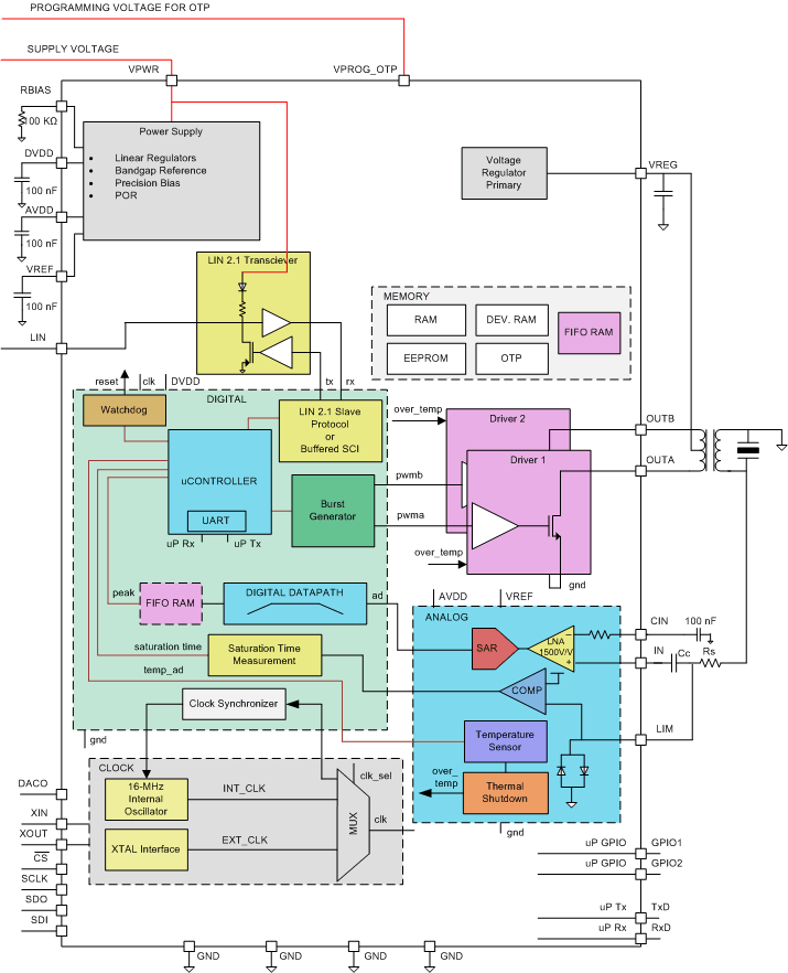
The PGA450-Q1 integrates power management, low-side drivers, analog front-end, digital datapath, and interface functions to form a full ultrasonic-sensor signal conditioning solution. The low-side drivers are programmed to drive a specific frequency that matches the external ultrasonic transducer. After transmitting, the same transducer receives the reflected echo signal. The analog front-end filters and amplifies this signal before storing the data in memory. The integrated 8051 microcontroller then processes this data to extract the useful information which typically includes how far away an object is from the transducer. At this point in the process, the information is transmitted through LIN, SCI, or UART.
7.2 Functional Block Diagram
7.3 Feature Description
7.3.1 Power Supply Block
The PGA450-Q1 uses three internal regulators (AVDD, DVDD, and VREF) as supplies for all of the internal circuits. The power-supply block also generates a precision voltage reference, current bias, and internal clock. The internal power-on-reset (POR) signal is released when the internal power supplies, voltage reference, current bias, and internal clock come into regulation.
Figure 7 shows the relationships of the power supplies and the POR signal in the PGA450-Q1 device.
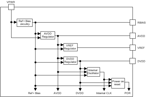 Figure 7. Power-Supply Block
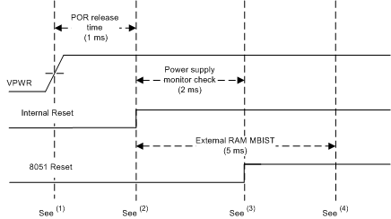
The PGA450-Q1 begins to power up when a voltage is applied to the VPWR pin. Figure 8 shows a typical power-up diagram. The power-up time is typically about 3 ms.
The PGA450-Q1 provides two power-control bits for enabling different analog blocks to manage the total current consumption of the device. On power up, the device is in the QUIET mode with only the 8051W and LIN transceiver turned on. All other analog blocks are disabled. Setting the ACTIVE_EN bit enables the low-side drivers required for bursting as well as the echo-processing circuitry that includes the LNA and the ADC. In addition, a separate control bit, VREG_EN, is provided to enable the VREG circuitry, which is used to charge the external capacitor used during bursting.
The AVDD pin can be used to source current for up to 5 mA for resistive loads, including the loads on the GPIO and Tx pins.
Table 1. Power Modes
| CONTROL BIT | DEFAULT | FUNCTION | |
|---|---|---|---|
| 1 | VREG_EN | Disabled | Enables the VREG circuitry that provides the 100-mA current to charge the external capacitor used during bursting |
| 2 | ACTIVE_EN(1) | Disabled | Enables the LNA, ADC, ADC REF, and other support circuitry related to burst generation and echo processing |
7.3.2 VREG
The PGA450-Q1 provides a regulated voltage output which, along with an external capacitor, can be used to drive the primary of the transformer used to excite the transducer. The VREG regulator provides a 100-mA current, sourced from VPWR, to charge the external capacitor. The user can select the desired VREG voltage by setting the VREG_SEL register to the appropriate value.
For VREG to be regulated to the selected voltage, VPWR must be at least 2 V above the selected VREG voltage.
The energy required for the burst comes from the external capacitor. The device has a VREG_READY status bit in the STATUS2 register to indicate when the capacitor is fully charged and has reached the regulation voltage.
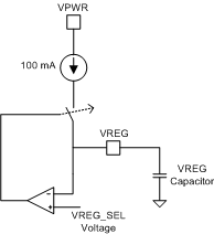 Figure 9. VREG Regulator
This block is disabled by default. Setting the VREG_EN bit in the PWR_MODE register to high, enables this regulator.
7.3.3 Clock
The clock block generates the system clock that is used in the generation of burst, communication, echo time measurement, and the microprocessor clock. Figure 10 shows the clock block in the PGA450-Q1.
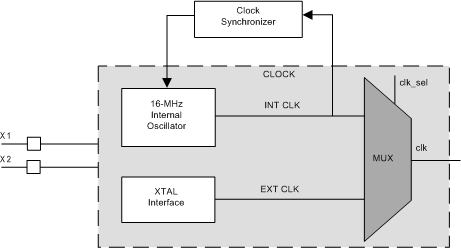 Figure 10. Clock Block in PGA450-Q1
The CLK signal provided to various blocks inside the device is derived from one of the following sources:
- Internal oscillator without synchronization with communication: in this mode, the internal oscillator output is the source for the system clock.
- Internal oscillator with synchronization with communication: in this mode, the internal oscillator output is corrected for inaccuracy using time measurements of the communication bus. This mode requires the implementation of CLOCK SYNCHRONIZER logic in the digital control block. The clock synchronizer uses the SYNC FIELD to measure the timer value and adjust the internal oscillator output.
- External crystal: in this mode, a 16-MHz external crystal is the source of the system clock.
The clock source is controlled by the CLK_SEL register. Table 2 lists the settings of the CLK_SEL bits and the corresponding clock mode.
Table 2. Clock Selection
| CLK_SEL BIT VALUES | CLOCK SOURCE |
|---|---|
| 0b00 | Internal clock. Ignore the synchronization pulse received on the LIN bus. |
| 0b01 | Internal clock. Process the synchronization pulse received on the LIN bus. |
| 0b10 | External crystal clock |
| 0b11 | Internal clock. Ignore the synchronization pulse received on the LIN bus. |
7.3.3.1 Clock Synchronizer Using the SYNC Field in the LIN Bus
The clock synchronizer block adjusts the internal oscillator based on a SYNC field in the LIN frame received in the communication line. The internal clock is trimmed to 16 MHz with ±4% tolerance in the TI factory.
The clock synchronizer improves the instantaneous accuracy of the internal oscillator frequency to 16 MHz ±0.5% using the LIN SYNC field, assuming an ideal LIN baud rate of 19.2 kBPS. The synchronization algorithm uses the time between two falling edges of the LIN SYNC field to adjust the internal oscillator.
The SYNC_COUNT is available for the 8051W to determine the effectiveness of the synchronization process based on the LIN SYNC field. That is, if the synchronization was effective, then the SYNC COUNT value should be close to 1667 ±8 counts.
This OSC SYNC value can also be updated by the 8051W microprocessor by setting the OVR bit in OSC_SYNC_CTRL ESFR.
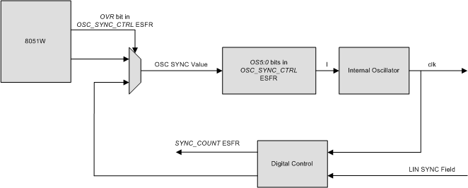 Figure 11. PGA450-Q1 Internal Clock Synchronization Control
Table 3 lists the value of OS<5:0> and the resulting change in frequency.
Table 3. OS<5:0> versus Delta System Clock Frequency
| OS<5:0> | Delta Frequency |
|---|---|
| 0 | –3.84 MHz |
| .. | .. |
| 31 | –120 kHz |
| 32 | 0 kHz |
| 33 | 120 kHz |
| .. | .. |
| 63 | 3.72 MHz |
NOTE
The clock synchronization feature is not available if the device is configured in SCI buffered mode. See the LIN 2.1 Slave and Buffered SCI section for details.
7.3.4 Low-Side Drive FETs
The PGA450-Q1 provides two low-side drivers for driving the primary of a transformer or an equivalent load. The Burst Generator section describes the control and drive modes for the low-side drive.
The low-driver block also has diagnostics. See the Diagnostics section for a description of the diagnostics.
Figure 12 shows the schematic of the low-side drive
 Figure 12. Low-Side Drive Block Diagram
7.3.5 Burst Generator
The burst generator block generates the high-frequency pulses used to drive the gates of the low-side FETs. The low-side FETs ultimately drive the transducer by modulating the primary of the transformer.
The PGA450-Q1 provides mode bits in the BURST MODE register (see the Burst Mode Register (offset = 0xB3) [reset = 0] section) to configure each low-side drive MOSFET in three possible drive modes.
The three possible drive modes are:
-
Single-ended:In this mode, one low-side switch is used to turn current on and off in the primary of the transformer. The rate of change of current in the primary generates a voltage in the secondary of the transformer, which is connected to the transducer.
-
Push-pull:In this mode, two low-side switches are used to turn current on and off in two primary coils in the transformer. The primary coils have the same number of turns. The rate of change of current in the primary generates a voltage in the secondary of the transformer, which is connected to the transducer. The direction of current in the primary coils generates voltages of opposite polarity in the secondary, effectively doubling the peak-to-peak voltage in the secondary.
-
8051W port drive:In this mode, the low-side switches are controlled through the an 8051W port pin.
Figure 13 shows the block diagram of the burst generator. The figure shows that the burst generator has a number of registers which the user software must configure.
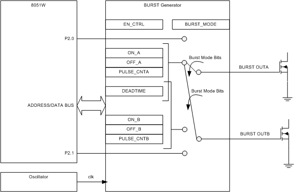 Figure 13. Burst Generator
The PGA450-Q1 provides 3 mode bits in the BURST MODE register to select from the five burst configurations available. Table 4 lists the modes of operation of the two low-side gate drives of the burst generator. For an understanding of the configurations, see Figure 14 and for an understanding of the waveforms, see Figure 15.
Table 4. Low-Side MOSFET Gate Drive Modes
Figure 14 shows the relationship of BURST_OUTx.
 Figure 14. Timing Diagram Showing the Usage of ON Register, OFF Register and PULSE COUNT Register Values
The relationship between the ONTIME, OFFTIME, and DEADTIME values in the push-pull configurations are shown in Figure 15.
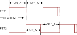 Figure 15. Timing Diagram Showing the Relationship Between ONTIME, OFFTIME, and DEADTIME Registers in the Push-Pull Configuration
Table 5 lists the 8051W port pins used to drive the OUTA and OUTB pins are listed in the 8051W drive mode.
Table 5. OUTA/OUTB Pin Map
| PGA450-Q1 PIN | 8051W PORT |
|---|---|
| OUTA | 2.0 |
| OUTB | 2.1 |
7.3.6 Low-Noise Amplifier
This block is the analog front-end that interfaces with the transducer directly. The echo signal is coupled through an external capacitor so that only the AC component of the transducer voltage is passed to the low-noise amplifier (LNA). The LNA outputs an amplified version of the transducer voltage with a DC offset that is equal to the mid-scale of the analog-to-digital converter (ADC).
The LNA gain is configurable by setting the LNA_GAIN1 and LNA_GAIN0 bits in the CONTROL_1 register to the appropriate values.
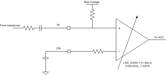 Figure 16. Low-Noise Amplifier
7.3.7 Analog-to-Digital Converter
The 12-bit successive approximation register (SAR) analog-to-digital converter converts the analog voltage from the echo-processing circuit into a digital word. The converted digital word is processed by the bandpass filter. The ADC is dedicated to the echo-processing signal path and is only enabled in active mode.
7.3.8 Digital Data Path
The digital datapath processes the AD sample to extract the peak profile of the echo. The output of the digital datapath is stored in the FIFO RAM.
Figure 17 shows the digital datapath.
 Figure 17. Digital Data Path
The digital datapath has the following components:
Each of the digital datapath components is described in the following subsections.
7.3.8.1 Bandpass Filter (BPF)
The echo signal is an amplitude-modulated signal with the underlying carrier frequency equal to the drive frequency of the ultrasonic transducer. The bandpass filter block allows frequencies near the drive frequency to pass to downstream signal blocks.
The bandpass filter is a second-order Butterworth IIR filter. The user can configure the center frequency and the bandwidth of the filter by writing specific values to coefficient registers BPF_B1, BPF_A2, and BPF_A3.
Table 7 lists the values (in hex) that must be written to the coefficient registers to realize a bandpass filter of specific center frequency and bandwidth (or Q).
NOTE
The stability of the filter is not assured if values other than those listed in Table 7 are written to the registers.
Table 6. Bandpass Filter Coefficient Values
| BW (kHz) | B1 (Hex) | A3 (Hex) |
|---|---|---|
| 4 | 32D | F9A5 |
| 4.5 | 392 | F8DD |
| 5 | 3F6 | F815 |
| 5.5 | 459 | F74D |
| 6 | 4BD | F687 |
| 6.5 | 520 | F5C1 |
| 7 | 582 | F4FB |
Table 7. Bandpass Filter Coefficient Values
| CF (kHz) | BW (kHz) | A2 (Hex) |
|---|---|---|
| 39 | 4 | F54A |
| 5 | F48B | |
| 6 | F3CD | |
| 7 | F311 | |
| 40 | 4 | F4E6 |
| 5 | F427 | |
| 6 | F36A | |
| 7 | F2AE | |
| 41 | 4 | F480 |
| 5 | F3C1 | |
| 6 | F304 | |
| 7 | F249 | |
| 42 | 4 | F417 |
| 5 | F358 | |
| 6 | F29C | |
| 7 | F1E1 | |
| 43 | 4 | F3AC |
| 5 | F2ED | |
| 6 | F231 | |
| 7 | F176 | |
| 44 | 4 | F33E |
| 5 | F280 | |
| 6 | F1C4 | |
| 7 | F10A | |
| 45 | 4 | F2CE |
| 5 | F210 | |
| 6 | F154 | |
| 7 | F09A | |
| 46 | 4 | F25B |
| 5 | F19E | |
| 6 | F0E2 | |
| 7 | F029 | |
| 47 | 4 | F1E6 |
| 5 | F129 | |
| 6 | F06E | |
| 7 | EFB5 | |
| 48 | 4 | F16E |
| 5 | F0B2 | |
| 6 | EFF7 | |
| 7 | EF3E | |
| 49 | 4 | F0F4 |
| 5 | F038 | |
| 6 | EF7E | |
| 7 | EEC5 | |
| 50 | 4 | F078 |
| 5 | EFBC | |
| 6 | EF02 | |
| 7 | EE4A | |
| 51 | 4 | EFF9 |
| 5 | EF3E | |
| 6 | EE84 | |
| 7 | EDCC | |
| 52 | 4 | EF78 |
| 5 | EEBD | |
| 6 | EE03 | |
| 7 | ED4C | |
| 53 | 4 | EEF4 |
| 5 | EE39 | |
| 6 | ED80 | |
| 7 | ECC9 | |
| 54 | 4 | EE6E |
| 5 | EDB4 | |
| 6 | ECFB | |
| 7 | EC44 | |
| 55 | 4 | EDE5 |
| 5 | ED2B | |
| 6 | EC73 | |
| 7 | EBBD | |
| 56 | 4 | ED5A |
| 5 | ECA1 | |
| 6 | EBE9 | |
| 7 | EB33 | |
| 57 | 4 | ECCD |
| 5 | EC14 | |
| 6 | EB5D | |
| 7 | EAA7 | |
| 58 | 4 | EC3D |
| 5 | EB85 | |
| 6 | EACE | |
| 7 | EA19 | |
| 59 | 4 | EBAB |
| 5 | EAF3 | |
| 6 | EA3D | |
| 7 | E988 | |
| 60 | 4 | EB16 |
| 5 | EA5F | |
| 6 | E9A9 | |
| 7 | E8F5 | |
| 61 | 4 | EA7F |
| 5 | E9C8 | |
| 6 | E913 | |
| 7 | E85F | |
| 62 | 4 | E9E6 |
| 5 | E930 | |
| 6 | E87B | |
| 7 | E7C7 | |
| 63 | 4 | E94B |
| 5 | E894 | |
| 6 | E7E0 | |
| 7 | E72D | |
| 64 | 4 | E8AD |
| 5 | E7F7 | |
| 6 | E743 | |
| 7 | E691 | |
| 65 | 4 | E80C |
| 5 | E757 | |
| 6 | E6A4 | |
| 7 | E5F2 | |
| 66 | 4 | E769 |
| 5 | E6B5 | |
| 6 | E602 | |
| 7 | E551 | |
| 67 | 4 | E6C4 |
| 5 | E610 | |
| 6 | E55E | |
| 7 | E4AD | |
| 68 | 4 | E61D |
| 5 | E569 | |
| 6 | E4B8 | |
| 7 | E407 | |
| 69 | 4 | E573 |
| 5 | E4C0 | |
| 6 | E40F | |
| 7 | E35F | |
| 70 | 4 | E4C7 |
| 5 | E415 | |
| 6 | E364 | |
| 7 | E2B5 |
7.3.8.2 Rectifier
The output of the bandpass filter is a signed number. The rectifier rectifies the output of the bandpass filter to create a positive number.
7.3.8.3 Peak Extractor
The peak extractor in the PGA450-Q1 is a simple moving-peak algorithm. Specifically, the output of the peak extractor is updated if the input to the peak extractor is greater than the previous output of the peak extractor. This algorithm is summarized in Equation 1.
where
- y is the output of the peak extractor
- x is the input to the peak extractor
- k is the discrete-time step
Figure 18 shows the peak extractor algorithm.
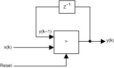 Figure 18. Peak Extractor
7.3.8.4 Downsample
The downsample block performs two functions:
- Generates the reset signal for the peak extractor shown in Figure 18.
- Generates the output.
The downsample rate can be configured by the user by writing to the downsample register. If the output of the peak extractor must be low-pass filtered before storing it in the FIFO, then the allowable values for the downsample register for the low-pass filter correctly are from 25 to 50; that is:
However, if the user does not need to low-pass filter the output before storing to the FIFO, then the user can configure the DOWNSAMPLE register value to any value between 1 and 63.
The downsample block has a counter which starts at 0 and counts up to the values programmed in the DOWNSAMPLE register. When the count reaches the value in the DOWNSAMPLE register, the counter inside the downsample block is reset to 0. Furthermore, the downsample block generates a reset to the peak extractor. This reset signal sets the output of the peak extractor to 0.
The data output rate of the downsample block is:
7.3.8.5 Low-Pass Filter
The output of the downsample block can be filtered by a low-pass filter. The low-pass filter in the PGA450-Q1 device is a first-order Butterworth IIR filter with a configurable cutoff frequency.
The user can configure the cutoff frequency of the filter by writing specific values to coefficient registers LPF_B1 and LPF_A2. Note that for the same desired cutoff frequency, the coefficient values depend on the configured DOWNSAMPLE register.
Table 8 lists the values (in hex) that must be written to the coefficient registers to realize a low-pass filter of a specific cutoff frequency. The stability of the filter is not assured if values other than those listed in the table are written to the registers.
Table 8. Low-Pass Filter Coefficient Values
| CUTOFF (kHz) | DOWNSAMPLE (Hex) | B1 (Hex) | A2 (Hex) |
|---|---|---|---|
| 0.5 | 19 | 4D7 | 7652 |
| 1A | 506 | 75F3 | |
| 1B | 536 | 7594 | |
| 1C | 565 | 7535 | |
| 1D | 595 | 74D7 | |
| 1E | 5C4 | 7479 | |
| 1F | 5F3 | 741B | |
| 20 | 622 | 73BD | |
| 21 | 650 | 7360 | |
| 22 | 67F | 7302 | |
| 23 | 6AD | 72A5 | |
| 24 | 6DC | 7249 | |
| 25 | 70A | 71EC | |
| 26 | 738 | 7190 | |
| 27 | 766 | 7134 | |
| 28 | 794 | 70D9 | |
| 29 | 7C1 | 707E | |
| 2A | 7EF | 7022 | |
| 2B | 81C | 6FC8 | |
| 2C | 84A | 6F6D | |
| 2D | 877 | 6F13 | |
| 2E | 8A4 | 6EB9 | |
| 2F | 8D1 | 6E5F | |
| 30 | 8FD | 6E05 | |
| 31 | 92A | 6DAC | |
| 32 | 957 | 6D53 | |
| 1.0 | 19 | 957 | 6D53 |
| 1A | 9B0 | 6CA1 | |
| 1B | A08 | 6BF0 | |
| 1C | A60 | 6B41 | |
| 1D | AB7 | 6A92 | |
| 1E | B0E | 69E5 | |
| 1F | B64 | 6937 | |
| 20 | BBA | 688B | |
| 21 | C10 | 67E0 | |
| 22 | C65 | 6736 | |
| 23 | CBA | 668C | |
| 24 | D0E | 65E4 | |
| 25 | D62 | 653C | |
| 26 | DB6 | 6495 | |
| 27 | E09 | 63EF | |
| 28 | E5B | 6349 | |
| 29 | EAE | 62A5 | |
| 2A | EFF | 6201 | |
| 2B | F51 | 615E | |
| 2C | FA2 | 60BC | |
| 2D | FF3 | 601B | |
| 2E | 1043 | 5F7A | |
| 2F | 1093 | 5EDA | |
| 30 | 10E2 | 5E3B | |
| 31 | 1132 | 5D9D | |
| 32 | 1180 | 5CFF | |
| 1.5 | 19 | D8C | 64E8 |
| 1A | E09 | 63EF | |
| 1B | E84 | 62F7 | |
| 1C | EFF | 6201 | |
| 1D | F79 | 610D | |
| 1E | FF3 | 601B | |
| 1F | 106B | 5F2A | |
| 20 | 1000 | 5E3B | |
| 21 | 1159 | 5D4E | |
| 22 | 11CF | 5C62 | |
| 23 | 1244 | 5B78 | |
| 24 | 12B8 | 5A90 | |
| 25 | 132C | 59A9 | |
| 26 | 139E | 58C4 | |
| 27 | 1410 | 57E0 | |
| 28 | 1481 | 56FD | |
| 29 | 14F2 | 561C | |
| 2A | 1562 | 553D | |
| 2B | 15D1 | 545E | |
| 2C | 163F | 5381 | |
| 2D | 16AD | 52A6 | |
| 2E | 171A | 51CC | |
| 2F | 1786 | 50F3 | |
| 30 | 17F2 | 501C | |
| 31 | 185D | 4F45 | |
| 32 | 18C8 | 4E70 | |
| 2.0 | 19 | 1180 | 5CFF |
| 1A | 121D | 5BC6 | |
| 1B | 12B8 | 5A90 | |
| 1C | 1352 | 595C | |
| 1D | 13EA | 582B | |
| 1E | 1481 | 56FD | |
| 1F | 1517 | 55D1 | |
| 20 | 15AC | 54A8 | |
| 21 | 163F | 5381 | |
| 22 | 16D1 | 525D | |
| 23 | 1762 | 513B | |
| 24 | 17F2 | 501C | |
| 25 | 1881 | 4EFE | |
| 26 | 190F | 4DE3 | |
| 27 | 199B | 4CCA | |
| 28 | 1A27 | 4BB3 | |
| 29 | 1AB1 | 4A9E | |
| 2A | 1B3A | 498B | |
| 2B | 1BC3 | 487A | |
| 2C | 1C4A | 476B | |
| 2D | 1CD1 | 465E | |
| 2E | 1D56 | 4553 | |
| 2F | 1DDB | 444A | |
| 30 | 1E5F | 4342 | |
| 31 | 1EE2 | 423C | |
| 32 | 1F64 | 4138 | |
| 2.5 | 19 | 153D | 5587 |
| 1A | 15F6 | 5415 | |
| 1B | 16AD | 52A6 | |
| 1C | 1762 | 513B | |
| 1D | 1816 | 4FD4 | |
| 1E | 18C8 | 4E70 | |
| 1F | 1978 | 4D10 | |
| 20 | 1A27 | 4BB3 | |
| 21 | 1AD3 | 4A59 | |
| 22 | 1B7F | 4903 | |
| 23 | 1C29 | 47AF | |
| 24 | 1CD1 | 465E | |
| 25 | 1D78 | 4511 | |
| 26 | 1E1D | 43C6 | |
| 27 | 1EC1 | 427E | |
| 28 | 1F64 | 4138 | |
| 29 | 2005 | 3FF5 | |
| 2A | 20A6 | 3EB5 | |
| 2B | 2145 | 3D77 | |
| 2C | 21E2 | 3C3B | |
| 2D | 227F | 3B02 | |
| 2E | 231A | 39CB | |
| 2F | 23B5 | 3897 | |
| 30 | 244E | 3764 | |
| 31 | 24E6 | 3633 | |
| 32 | 257E | 3505 | |
| 3.0 | 19 | 18C8 | 4E70 |
| 1A | 199B | 4CCA | |
| 1B | 1A6C | 4B28 | |
| 1C | 1B3A | 498B | |
| 1D | 1C07 | 47F3 | |
| 1E | 1CD1 | 465E | |
| 1F | 1D99 | 44CE | |
| 20 | 1E5F | 4342 | |
| 21 | 1F23 | 41BA | |
| 22 | 1FE5 | 4036 | |
| 23 | 20A6 | 3EB5 | |
| 24 | 2164 | 3D38 | |
| 25 | 2221 | 3BBE | |
| 26 | 22DC | 3A47 | |
| 27 | 2396 | 38D4 | |
| 28 | 244E | 3764 | |
| 29 | 2505 | 35F7 | |
| 2A | 25BA | 348D | |
| 2B | 266E | 3325 | |
| 2C | 2720 | 31C0 | |
| 2D | 27D1 | 305E | |
| 2E | 2881 | 2EFE | |
| 2F | 292F | 2DA1 | |
| 30 | 29DD | 2C46 | |
| 31 | 2A89 | 2AED | |
| 32 | 2B35 | 2997 | |
| 3.5 | 19 | 1C29 | 47AF |
| 1A | 1D14 | 45D9 | |
| 1B | 1DFC | 4408 | |
| 1C | 1EE2 | 423C | |
| 1D | 1FC5 | 4076 | |
| 1E | 20A6 | 3EB5 | |
| 1F | 2184 | 3CF8 | |
| 20 | 2260 | 3B41 | |
| 21 | 2339 | 398D | |
| 22 | 2411 | 37DE | |
| 23 | 24E6 | 3633 | |
| 24 | 25BA | 348D | |
| 25 | 268B | 32E9 | |
| 26 | 275B | 314A | |
| 27 | 2829 | 2FAE | |
| 28 | 28F5 | 2E15 | |
| 29 | 29C0 | 2C80 | |
| 2A | 2A89 | 2AED | |
| 2B | 2B51 | 295E | |
| 2C | 2C17 | 27D2 | |
| 2D | 2CDC | 2648 | |
| 2E | 2DA0 | 24C0 | |
| 2F | 2E62 | 233C | |
| 30 | 2F23 | 21B9 | |
| 31 | 2FE4 | 2039 | |
| 32 | 30A3 | 1EBB | |
| 4.0 | 19 | 1F64 | 4138 |
| 1A | 2066 | 3F35 | |
| 1B | 2164 | 3D38 | |
| 1C | 2260 | 3B41 | |
| 1D | 2358 | 3950 | |
| 1E | 244E | 3764 | |
| 1F | 2541 | 357E | |
| 20 | 2632 | 339D | |
| 21 | 2720 | 31C0 | |
| 22 | 280C | 2FE8 | |
| 23 | 28F5 | 2E15 | |
| 24 | 29DD | 2C46 | |
| 25 | 2AC2 | 2A7B | |
| 26 | 2BA6 | 28B4 | |
| 27 | 2C88 | 26F0 | |
| 28 | 2D68 | 2530 | |
| 29 | 2E46 | 2373 | |
| 2A | 2F23 | 21B9 | |
| 2B | 2FFF | 2002 | |
| 2C | 30D9 | 1E4E | |
| 2D | 31B2 | 1C9D | |
| 2E | 3289 | 1AED | |
| 2F | 3360 | 1940 | |
| 30 | 3435 | 1796 | |
| 31 | 350A | 15ED | |
| 32 | 35DD | 1446 |
7.3.8.6 Datapath Output Format Control
The output of the datapath is stored in the ECHO DATA register. The output of the datapath register is updated at the rate determined by the value in the DOWNSAMPLE register.
The output of the digital datapath is also stored in the FIFO RAM. The user can configure the data stored in the FIFO RAM by writing values to the mode bits in the FIFO control (FIFO_CTRL) register.
Table 9 lists the output format of the digital datapath that is stored in the FIFO.
Table 9. Digital Datapath Output Format
| MODE BITS | OUTPUT FORMAT | DESCRIPTION |
|---|---|---|
| 0b00 | 12 bits | All 12 bits of the digital datapath output are stored in the FIFO. Note that storing 12 bits consumes 2 bytes of the FIFO RAM. |
| 0b01 | 8 most-significant bits | The upper 8 bits of the 12-bit digital datapath output are stored in the FIFO. |
| 0b10 | 8 least-significant bits | The lower 8 bits of the 12-bit digital datapath output are stored in the FIFO, if all the upper 4 bits of the digital datapath output are 0s. However, if one of the upper 4 bits of the digital datapath is 1, then 0xFF is stored to the FIFO. |
| 0b11 | 8 middle bits | Bits 10 through 3 of the 12-bit digital datapath output are stored in the FIFO, if the upper 2 bits of the digital datapath output are 0s. However, if one of the upper 2 bits of the digital datapath is 1, then 0xFF is stored to the FIFO. |
7.3.8.7 Datapath Activation and Blanking Timer
The digital datapath calculations can be enabled or disabled using the ECHO_EN bit in the enable control (EN_CTRL) register. When the ECHO_EN bit is set to 0, the digital datapath is disabled; that is, the datapath does not perform the calculations and does not update the FIFO RAM. Furthermore, the history of the band-pass and low-pass filters is reset to 0.
When the user sets ECHO_EN to 1, the digital datapath begins the computation. However, the output of the datapath does not immediately start filling the FIFO RAM. Rather, the output of the digital datapath is updated into the FIFO RAM when the user-configured BLANKING_TIMER value has expired.
The user-configurable BLANKING_TIMER register is an 8-bit-register with 16-µs resolution per bit. In other words, the user can set the blanking timer value from 0 µs to 4.08 ms in steps of 16 µs.
Figure 19 shows the state of the digital datapath based on the enable or disable state of ECHO_EN and the BLANKING_TIMER register value.
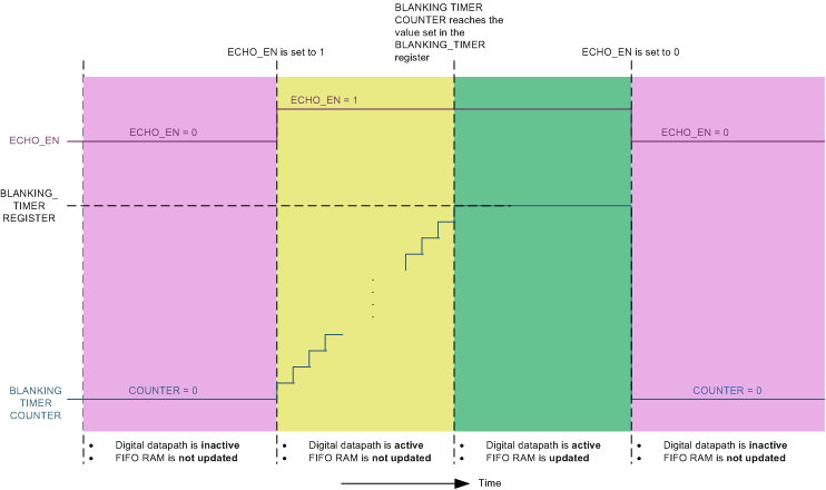 Figure 19. States of Digital Datapath
7.3.8.8 Digital Datapath Output Mode
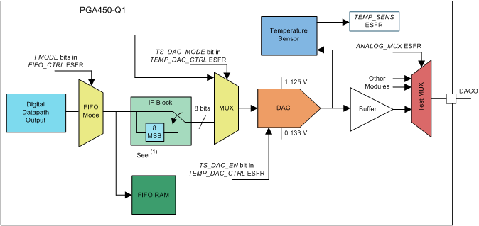
The digital datapath output is available in the analog-voltage mode on the DACO pin with the following constraints:
- The DAC is an 8-bit DAC. The DAC output works only in the 8-bit MSB, 8-bit LSB, or 8-bit middle-significant-bits modes of the digital datapath output.
- The DAC output voltage range is 0.133 V to 1.125 V with 8-bit resolution. The digital datapath output is directly scaled to the analog output voltage in this range.
- The DAC output voltage resolution is 1 / 255 V.
- An external amplifier or buffer may be needed before the output of the DAC can be used to drive a load or viewed on a scope.
- The ANALOG_MUX ESFR is used to control the availability of the DAC output on DACO pin. The reset state of the DACO is NONE which means that no internal signal is available until after POR.
- When the digital datapath output on DACO is enabled, the temperature sensor register (TEMP_SENS) is not updated.
To enable the temperature sensor or the digital datapath output, the TS_DAC_EN bit in TEMP_DAC_CTRL ESFR must be set to 1. The TS_DAC_mode bit determines whether the DAC is used for the temperature sensor or the digital datapath output.
7.3.9 Transducer Saturation Time
The transducer saturation block is used to measure the saturation time of the transducer. The measurement is based on the voltage at the LIM pin of the PGA450-Q1.
The transducer saturation time is defined as the time from when the SAT_EN bit in the enable control (EN_CTRL) register is set to 1 to the time when the voltage at LIM falls below the programmable threshold and stays below that threshold for the programmable deglitch time.
Figure 21 shows the block diagram of the transducer saturation-time measurement block. The saturation-time measurement is accomplished with the following registers.
- EN_CTRL register — set the SAT_EN bit.
- CONTROL_1 register — set the saturation threshold with the SAT_SEL1 and SAT_SEL0 bits
- SAT_DEGLITCH register (the saturation deglitch time register) — 8 bits at 2 µs resolution
- SAT_TIME register (the saturation time capture register) — 8 bits at 16 µs
- STATUS2 register — set the SAT_DONE bit
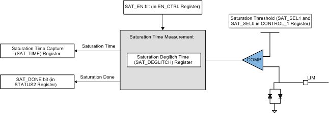 Figure 21. Transducer Saturation-Time Measurement Block
Figure 22 shows the timing diagram of the saturation-time measurement. The figure shows that an internal saturation timer starts when the SAT_EN bit in the EN_CTRL register is set to 1. The saturation-time measurement block then monitors only the positive voltage on the LIM pin. When this voltage goes below the programmed saturation threshold, the saturation-time deglitch timer is started.
NOTES:
- When the deglitch timer reaches the programmed deglitch time in the SAT_DEGLITCH register, the value in the internal saturation timer is captured into the SAT_TIME register and the SAT_DONE bit is set to 1.
- If the voltage at the LIM pin does not go below the programmed threshold after the SAT_EN bit is set to 1, then the SAT_DONE bit remains at 0. In this case, the maximum value of the SAT_TIME register is 0xFF.
- Setting the SAT_EN bit to 0 resets the SAT_TIME register to 0 and sets the SAT_DONE bit to 0.
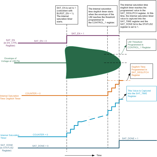 Figure 22. Timing Diagram Showing the Measurement of Transducer Saturation Time
7.3.10 Temperature Sensor
The PGA450-Q1 has an on-chip temperature sensor that provides a signed 8-bit 2s-complement output (MSB is the sign bit) with code 0 corresponding to 30°C. The temperature sensor has a typical gain of 1.75°C / code. The temperature sensor is disabled by default. The TS_DAC_EN bit in the TEMP_DAC_CTRL register must be set to enable the temperature sensor. The conversion time is typically 1.4 ms.
Equation 4 is the nominal equation for the temperature in °C.
7.3.11 Free-Running Timer
The PGA450-Q1 includes a 16-bit free-running timer that operates at a resolution of 1 µs. This timer can be used to synchronize echo transit times between two different PGA450-Q1 devices by the master ECU in triangulation applications.
This timer starts from a reset value of 0 at POR and counts up. When the timer values reaches 0xFFFF, the timer rolls over to 0x0000.
The value of the free-running timer is not visible to the 8051W. However, the instantaneous value of the free-running timer can be captured into the free-running timer (FRT) capture ESFR by setting the CAP_FR_TIMER bit in the ENABLE CONTROL register to 1.
The FRT ESFR is a shadow of the free-running timer. The shadow register is not updated continuously. To copy the current value of the free-running timer into the ESFR, do the following:
- Write a 1 to the CAP_FR_TIMER bit in the EN_CTRL register.
- Read the FRT register.
See the Register Maps section for descriptions of the registers.
NOTE
The reason for implementing the FRT register as a shadow register is to allow the reading of the MSB and LSB coherently. The transfer from the free-running timer value to the FRT register is a 16-bit transfer and it is coherent. Because the 8051 can read only 1 byte at a time, coherency is maintained between two MSB and LSB reads of the FRT register because the FRT register value does not change between the reads of the MSB and LSB.
7.3.12 GPIOs
The GPIOx pins on the PGA450-Q1 can be used as either general-purpose inputs and outputs (I/Os) or can be used as I/Os for specific functionality.
In the general-purpose I/Os mode, the GPIOx pins are connected to specific 8051W port pins. User software can be used to control the state of the device pins by controlling the appropriate I/O port SFRs in the 8051W. Table 10 lists the mapping of the PGA450-Q1 GPIOx pins to specific 8051W ports.
Table 10. GPIOx Pin Map
| PGA450-Q1 Pin | 8051W PORT |
|---|---|
| GPIO1 | 3.4 |
| GPIO2 | 3.5 |
7.3.13 8051W UART
The TxD and RxD pins on the PGA450-Q1 are connected to the 8051W UART. These two pins can be used either for software debugging or for implementing application-specific protocols.
Table 11. TxD and RxD Pin Functionality
| PGA450-Q1 Pin | 8051W PORT |
|---|---|
| TxD | 3.1 |
| RxD | 3.0 |
7.3.14 8051 WARP Core
The 8051 WARP core is an exceptionally high-performance version of this popular 8-bit microcontroller, requiring just 2 clocks per machine cycle rather than the 12 clocks per cycle of the industry-standard device, while keeping functional compatibility with the standard part. The 8051W core in the PGA450-Q1 includes two 16-bit timers and a serial interface.
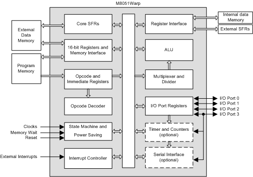 Figure 23. 8051W Core
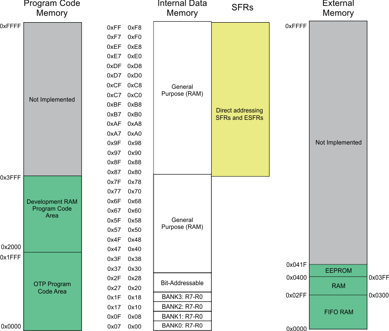
7.3.15 Memory
Table 12 lists the PGA450-Q1 memory types.
Table 12. Memory
| MEMORY | SIZE | DESCRITPTION |
|---|---|---|
| FIFO_RAM(1) | 768 bytes | Digital datapath output |
| Scratchpad RAM | 256 bytes | Used for software variables |
| OTP | 8K bytes | Program code |
| EEPROM | 32 bytes | Configuration data |
| DEVELOPMENT RAM | 8K bytes | Program code during development |
7.3.15.1 FIFO Memory for Digital Datapath Output
The FIFO memory is volatile RAM memory. The output of the digital datapath is stored in the FIFO memory.
The FIFO memory is memory-mapped to the 8051W external memory address space. The contents of the FIFO memory are accessible to the 8051W core.
The FIFO memory is a dual-port RAM; that is, that the 8051W can read the FIFO contents while the digital datapath is filling the memory.
The FIFO memory also has a FIFO pointer, which is stored in the FIFO_POINTER register. The FIFO pointer behavior is as follows:
- The FIFO pointer has the address of the last FIFO byte that was filled by the digital datapath.
- If the digital datapath has been configured to output data in 12-bit format, the FIFO pointer value increases by 2.
- If the digital datapath outputs data in 8-bit format, the FIFO pointer value increases by 1.
The FIFO pointer is reset to 0 at power up. Similarly, when the ECHO_EN bit in the EN_CTRL register is set to 1, the FIFO pointer value is reset to 0. However, the FIFO memory contents are not cleared to 0.
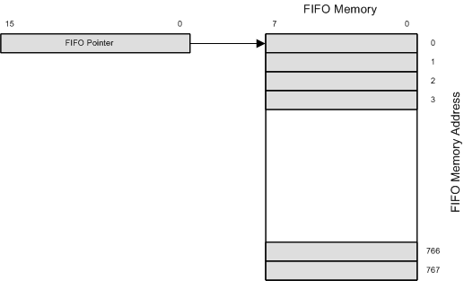 Figure 24. FIFO Memory Organization
7.3.15.2 OTP Memory for Program
The programming voltage for the OTP memory must be provided externally, because the device does not have a voltage regulator to generate the OTP programming voltage. This voltage must be provided on the VPROG_OTP pin.
7.3.15.2.1 OTP Security
The PGA450-Q1 provides the ability to LOCK the OTP. The OTP memory cannot be read or programmed through the SPI. This feature is called OTP security.
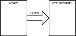 Figure 25. Connection Between the 8051W Core and OTP Security Block
The following is the procedure to LOCK and UNLOCK the OTP
- To LOCK the OTP memory, 8051W P0 should be set to 0xAA in software.
- To UNLOCK the OTP memory, 8051W P0 should be set to 0x00 in software.
NOTE
- Writing to P0 immediately after the 8051W reset is deasserted (immediately after the 8051W starts running software) is recommended.
- When the OTP memory is in LOCK state, the 8051W processor has access to OTP memory; that is, program execution can continue.
- If the 8051W processor is put in the reset state after a LOCK instruction in software has been executed, the OTP memory cannot be accessed through the SPI.
7.3.15.2.2 OTP Programming
Both the 8051W microprocessor and the SPI can access the 8K OTP memory. The 8051W has read access only. The SPI has read access and program access.
Prior to starting the OTP programming process, raising the VPROG_OTP pin on the PGA450-Q1 to 8 V is required. When the voltage on this device pin reaches this level, the OTP programming mode is enabled.
NOTE
The OTP programming voltage should not be connected to the pin for an extended period of time.
CAUTION
Do not power up OR power down the PGA450-Q1 with the VPROG_OTP pin set to 8 V, this may cause unrecoverable corruption to the OTP data.
Programming of the OTP must be done one address at a time. Each address can only be programmed once. After an address is programmed, it cannot be programmed again. Programming a section of the OTP address space and then programming an additional section of OTP address space at a later time is possible.
To program a byte of OTP, four bytes must be sent through SPI. The first byte is 0x07 indicating an OTP write operation. The next 2 bytes contain the address of the target OTP location and the last byte contains the data.
There should be at least 100 µs between two successive OTP write instructions. This time is needed to ensure the proper programming of the OTP cell. Violation of this might cause data retention issues for the OTP memory during the lifetime of the device. With a 4-MHz SCK frequency, it takes approximately 1 s to program the entire 8K address space of the OTP.
The following is the OTP memory programming procedure:
- After power up, set the VPROG_OTP pin to 8 V.
- Send an OTP write command through the SPI.
- The CS pin is set to HIGH at least 100 µs for the OTP programming process to complete. Do not perform any SPI write operations to the OTP during the OTP programming process.
- Repeat Steps 2 and 3 until all desired OTP addresses have been programmed.
- Before powering down the PGA450-Q1 device, disconnect the 8-V supply to VPROG_OTP pin.
7.3.15.3 EEPROM Memory for Data
Figure 26 shows the EEPROM structure in the PGA450-Q1 device. The EEPROM structure in PGA450-Q1 includes volatile cache. The cache has one-to-one mapping with the nonvolatile EEPROM memory cells. The EEPROM cache is mapped into the external memory space of the 8051W memory map.
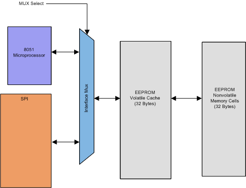 Figure 26. Structure of EEPROM Interface
7.3.15.3.1 EEPROM Memory Organization
7.3.15.3.1.1 EEPROM Cache
The EEPROM cache serves as temporary storage of data being transferred to or from EEPROM. Data transferred to the EEPROM cache from either SPI or from the M8051 is byte-addressable, and one byte at time can be written to or read from the EEPROM cache. Selection of the EEPROM cache interface is determined by the internally generated MUX-select bit. The MUX-select bit is by default set to 8051W access. The EEPROM cache is accessible to the SPI when the 8051W is put in reset in the test mode.
When programming to EEPROM through the SPI, the EEPROM cache holds the programming data for the amount of time necessary to complete the EEPROM programming process.
7.3.15.3.1.2 EEPROM Memory Cells
The EEPROM memory cells are nonvolatile. The contents of the cache are programmed into the EEPROM when the 8051W requests the programming. The cache is loaded with the contents of the EEPROM memory cells at power up.
7.3.15.3.2 Programming EEPROM Through the 8051W and SPI
The following is the EEPROM memory programming procedure:
- Write data to EEPROM cache
- Use the 8051W MOVX assembly instruction to place data in external memory addresses 0x0400 through 0x041F.
- Write a 1 to the WRITE bit in the EE_CTRL register.
- Continuously poll the EE_STATUS bit in EE_CTRL register for the programming status. The EEPROM programming requires 70 ms to complete.
7.3.15.3.3 Reloading From EEPROM Cells Through the 8051W and SPI
The following is the reloading procedure:
7.3.16 LIN 2.1 Slave and Buffered SCI
The PGA450-Q1 implements the LIN 2.1 compliant physical layer. This physical layer can be used to communicate data between the PGA450-Q1 and the master ECU.
The PGA450-Q1 can be configured to operate in the LIN 2.1 slave-protocol mode or SCI buffered mode. If the device is configured in LIN 2.1 slave-protocol mode, then the protocol layer described in Section 2.1 of the LIN 2.1 specification must be used to communicate with the PGA450-Q1. The device can only be configured as a slave; that is, the PGA450-Q1 cannot be used as a master.
The LIN 2.1 slave protocol implemented in PGA450-Q1 has the following exceptions:
- No wake-up (Section 2.6.2 of LIN 2.1). The device cannot be put to sleep and be woken through the LIN.
- No transport layer in digital logic (Section 3 of LIN 2.1)
- No node configuration and identification services in digital (Section 4 of LIN 2.1)
- No diagnostic layer in digital logic (Section 5 of LIN 2.1)
- Communication baud rate is fixed at 19.2 kBPS. That is, the device baud rate is not configurable.
The PGA450-Q1 can also be configured to operate in SCI buffered mode. In this mode, no specific protocol is needed to communicate with the PGA450-Q1. The user has the choice to implement the protocol in software. The device provides the ability either to transmit or to receive 8 bytes of data without any intervention from 8051W software.
The user selects either LIN 2.1 slave mode or SCI buffered mode by setting the LIN_SCI bit in the LIN_SCI_SEL register. If the LIN_SCI bit is changed from LIN mode to SCI mode or vice versa, the communication protocol is reset.
7.3.16.1 Physical Layer
The physical layer inside the PGA450-Q1 is compliant with the LIN 2.1 specification. Figure 27 shows the line driver and receiver schematic illustrated in the LIN 2.1 specification. The inner dashed box in Figure 27 identifies the section that has been implemented in the PGA450-Q1.
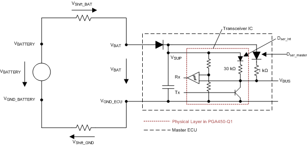
Figure 28 shows the schematic of the LIN 2.1 physical layer in PGA450-Q1. This figure infers that the PGA450-Q1 implements the LIN 2.1 slave physical layer.
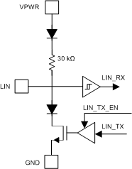 Figure 28. LIN Physical Layer in the PGA450-Q1
7.3.16.2 LIN Slave Mode
This section describes the LIN slave protocol mode of operation of the PGA450-Q1.
7.3.16.2.1 LIN Frame
This peripheral handles the LIN 2.1 frames shown in Figure 29. The LIN 2.1 frame has a break field, sync field, PID field, data fields, and checksum field.
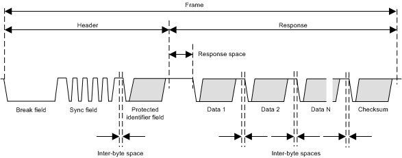 Figure 29. LIN Frame From the LIN 2.1 Specification
Figure 30 shows the LIN byte field. This figure shows that the LIN byte field has 1 start bit and 1 stop bit. The least-significant bit (LSB) is transmitted first.
 Figure 30. LIN Byte Field From the LIN 2.1 Specification
 Figure 31. LIN Break Field From the LIN 2.1 Specification
A break field is always generated by the master task (in the master node) and it shall be at least 13 nominal bit times of dominant value, followed by a break delimiter.
 Figure 32. LIN Sync Field From the LIN 2.1 Specification
Sync is a byte field with the data value 0x55.
7.3.16.2.2 LIN Registers
Figure 33 shows all the registers associated with the LIN peripheral. The LIN PID, RX DATA0–7 and TX DATA0–7 have unique registers associated with them.
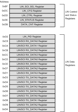 Figure 33. LIN Registers
NOTE
The PGA450-Q1 LIN slave protocol does not decode the LIN PID registers. The decoding logic for the PID registers must be implemented in 8051W software.
7.3.16.2.3 LIN Interrupts
Figure 34 shows the four interrupts that the LIN slave protocol generates. These interrupts are:
-
SYNC interrupt: This interrupt is generated by the LIN slave protocol when the SYNC field is received. Note that the SYNC field interrupt is generated regardless of whether the subsequent LIN frame fields are received. Thus, the customers can use the BREAK+SYNC fields to synchronize the internal clock and use other protocols for communication.
-
PID interrupt: This interrupt is generated by the LIN slave protocol when the PID is received and the PID does not have a parity error.
-
Rx interrupt: This interrupt is generated by the LIN slave protocol when the PGA450-Q1 receives the LIN data. The interrupt is generated only when the checksum is received and the checksum has no errors. The device performs the enhanced checksum calculation. According to the LIN 2.1 specification, the enhanced checksum is the checksum calculation over the data bytes and the protected identifier byte.
-
Tx interrupt: This interrupt is generated by the LIN slave protocol when the PGA450-Q1 transmits data. The interrupt is generated at the end of the checksum transmission.
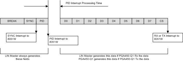 Figure 34. LIN Interrupts
The PID interrupt processing shown in Figure 34 is for a transmit message.
7.3.16.2.4 LIN Slave Configuration
The LIN slave in the PGA450-Q1 is configurable. This section describes the available configurations. These configurations are not applicable if the PGA450-Q1 is set up to operate in SCI buffered mode.
The LIN configuration register, LIN_CFG, is used to configure the LIN slave in the PGA450-Q1. The following sections describe the possible configurations.
7.3.16.2.4.1 LIN Frame-Control Configuration
The PGA450-Q1 has three bits that control the behavior of the PGA450-Q1 when a LIN frame is received.
-
IGNORE_DIAG: This bit controls the mode of operation of the LIN slave controller when the PID is received.
If this bit is set to 0, then the LIN slave controller waits for data bytes after the PID field in the LIN frame is received.
If this bit is set to 1, then the LIN slave controller finishes the current frame after the PID is received and waits for the next LIN frame.
-
HOLD: This bit determines whether the LIN frame received by PGA450-Q1 is processed or ignored.
If this bit is set to 1 (which is the power ON reset state), then the received LIN frame is ignored.
If this bit is set to 0, then the received LIN frame is not ignored.
-
CS_METHOD: This bit controls whether the checksum is classic checksum or enhanced checksum.
If this bit is set to 0 (which is power ON reset state), the LIN protocol calculates and validates the checksum using the classic checksum method.
If this bit is set to 1, the LIN protocol calculates and validates the checksum using the enhanced checksum method.
7.3.16.2.4.2 LIN Timing-Control Configuration
The PGA450-Q1 has two bits that control the various timing parameters of the LIN frame.
-
INTERBYTE_SPACE: This bit controls the duration of the time between the data fields when PGA450-Q1 is transmitting data.
If this bit is set to 0, then the interbyte space is equal to 1 bit.
If this bit is set to 1, then the interbyte space is equal to 2 bits.
-
BIT_TOL:This bit controls the tolerance of bit time that is used in the LIN frame timing diagnostics.
If this bit is set to 0, the bit time tolerance is 15% of the bit time determined during the LIN SYNC field.
If this bit is set to 1, the bit time tolerance is 30% of the bit time determined during the LIN SYNC field.
7.3.16.2.5 LIN Slave-Protocol State Machine
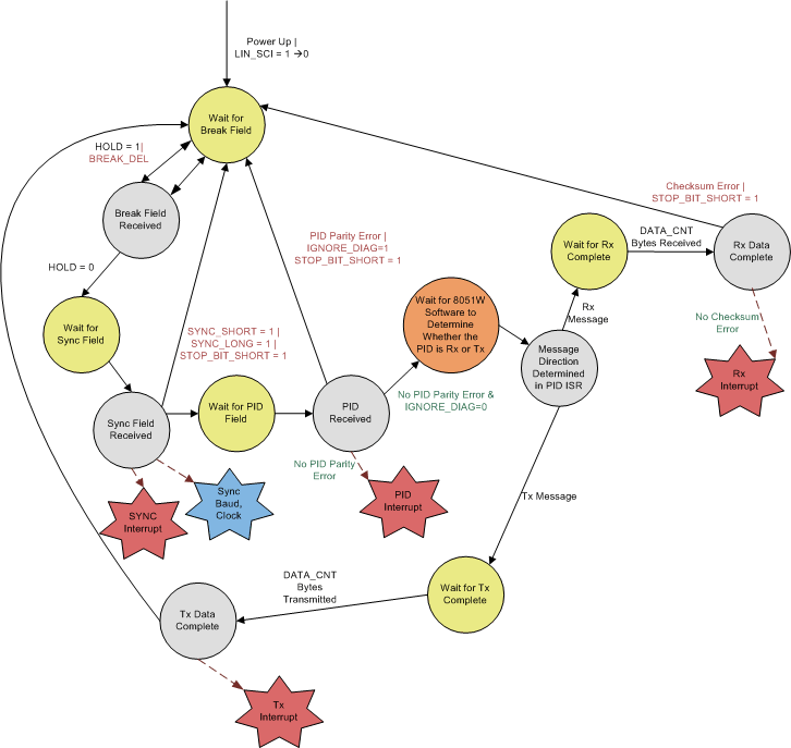
Figure 35 shows the LIN slave-protocol state machine implemented inside PGA450-Q1. The figure shows that the protocol enters the Wait-for-Break-Field state on power up. When the master sends the break field, the state machine transitions into the Wait-for-Sync-Field state only if the HOLD bit in the LIN_CFG register is set to 0. Otherwise, the LIN protocol return to the Wait-for-Break-Field state.
After the sync field is received, the state machine generates the SYNC field interrupt and transitions into the Wait-for-PID-Field state. After the PID field is received, the PID parity is checked. If the parity has an error, then the state machine transitions back to the Wait-for-Break-Field state. If there is no parity error, then the state machine generates the PID interrupt to the 8051W.
The user must write software to service the PID interrupt. In the PID interrupt service routine, the user determines whether the received PID corresponds to Rx message or Tx message.
In the case of an Rx message, the state machine waits for all the data bytes to be received. The number of data bytes received is determined by the value in the DATA_CNT register. When all the data bytes are received, then the state machine calculates the checksum. If the calculated checksum matches the received checksum, then the state machine generates an Rx interrupt to the 8051W. Otherwise, the state machine transitions back to Wait-for-Break-Field state.
In the case of a Tx Message, the state machine calculates the checksum based on the data after the 8051W loads the transmit buffers and the DATA_CNT register. At the end of frame transmission (that is, when the checksum is transmitted), the state machine generates a Tx interrupt to the 8051W.
NOTE:
When the LIN_SCI bit is changed from LIN mode to SCI mode while the LIN mode is in any of the states, the LIN state machine goes to the Wait-for-Break-Field state.7.3.16.2.6 LIN Slave Protocol Rx
If the PID field corresponds to an Rx message, the following are the steps to receive a LIN message.
In the PID interrupt service routine, do the following:
- Load the DATA_CNT ESFR with the expected number of Rx data bytes.
- Set the RX_TX bit in the LIN_CTRL ESFR to 0 to receive a message.
In the Rx interrupt service routine, do the following:
- Transfer data from the RX_DATA buffers to RAM.
See the ESFR Registers section for details on the ESFRs.
7.3.16.2.7 LIN Slave Protocol Tx
If the PID field corresponds to a Tx message, the following are the steps to transmit a LIN message.
In the PID interrupt service routine, do the following:
- Load DATA_CNT ESFR with the number of data bytes to be transmitted.
- Load TX_DATA buffers with the data that is to be transmitted.
- Set the RX_TX bit in LIN_CTRL ESFR to 1 to transmit a message.
When the Tx interrupt service routine is called, the message transmission is complete. Nothing is required in the Tx interrupt service routine.
See the ESFR Registers section for details on the ESFRs.
NOTE
The LIN PID will be received and stored in the LIN_PID ESFR. This register will be cleared when the LIN message transmission or reception is complete. Therefore, to retain the value of the LIN_PID, the user has to copy the value of the ESFR to a RAM variable.
7.3.16.2.8 LIN Slave Status
The PGA450-Q1 has a LIN status (LIN_STATUS) register that has the error status of the received LIN frame.
This LIN_STATUS register can be cleared at any time by setting the CLR_ERR bit in the LIN_CFG register to 1.
7.3.16.2.8.1 LIN Slave Framing Error Status
The LIN_STATUS register in the PGA450-Q1 has the following bits that reflect any framing errors in the received LIN message:
-
CHECKSUM:This bit is set to 1 if the received checksum does not match the calculated checksum.
-
PARITY: This bit is set to 1 if the received PID has a parity error.
7.3.16.2.8.2 LIN Slave Timing Error Status
The LIN_STATUS register in the PGA450-Q1 has bits that reflect any LIN timing errors in the received LIN message. The timing errors are based on Figure 36.
Table 13 lists the various timing errors in the received LIN message that are detected by the PGA450-Q1.
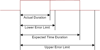 Figure 36. LIN Timing-Error Diagram
Table 13. LIN Timing Errors(1)
| ERROR BIT | DESCRIPTION | LOWER ERROR LIMIT | UPPER ERROR LIMIT |
|---|---|---|---|
| STOP_BIT_SHORT | STOP bit received in PID or data bytes is shorter than expected. | 52 µs × (1 – BIT_TOL) | |
| SYNC_SHORT | SYNC field duration is shorter than expected. | 485 µs | |
| SYNC_LONG | SYNC field duration is longer than expected. | 555 µs | |
| BREAK_DEL | BREAK FIELD delimiter is shorter than expected. | 52 µs × (1 – BIT_TOL) |
7.3.16.3 SCI Buffered Mode
In the SCI buffered mode, the PGA450-Q1 does not implement any special frame or protocol. Up to 8 bytes can be received and transmitted without any 8051W software intervention. That is, the software either reads (in the case of receive) from the Rx data buffer or writes (in the case of transmit) to the Tx data buffer the appropriate number of bytes.
The DATA_CNT ESFR determines the buffer length. When data is received by the device, SCI generates an Rx data interrupt only after the number of bytes specified in DATA_CNT register is received.
7.3.16.3.1 SCI Buffered-Mode State Machine
Figure 37 shows the SCI buffered-mode state machine. If both the external device and the 8051W try to send data at the same time, a bus conflict occurs. This bus contention is not detected inside the PGA450-Q1.
If the external device sends more than 8 bytes (corresponding to the buffer length), then the data in the Rx data buffer is overwritten. Therefore, the 8051W has not had a chance to read the previous data in the buffer, so the data is lost.
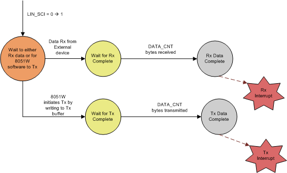 Figure 37. SCI Buffered-Mode State Machine
7.3.16.3.2 SCI Buffered-Mode Rx
The following are the steps to receive data on SCI:
- In software, do the following:
- Load DATA_CNT ESFR with the expected number of Rx data bytes.
- Set the RX_TX bit in LIN_CTRL ESFR to 0 to Rx a message.
- In the Rx interrupt service routine, do the following:
- Transfer data from the RX_DATA buffers to RAM.
7.3.16.3.3 SCI Buffered-Mode Tx
The following are the steps to transmit data on SCI:
- In software, do the following:
- Load DATA_CNT ESFR with the number of data bytes to be transmitted.
- Load TX_DATA buffers with the data to be transmitted.
- Set the SCI_TX_EN bit in DP_SCI_CTRL ESFR to 1 to Tx a message.
- Set the RX_TX bit in LIN_CTRL ESFR to 1 to Tx a message.
- When the Tx interrupt service routine is called, the message transmission is complete. Nothing is required in the Tx interrupt service routine.
NOTE
DATA_CNT in SCI buffered mode: The minimum value for DATA_CNT in SCI buffered mode is 2; that is, when the device is configured to operate in SCI buffered mode, the device can receive or transmit a minimum of 2 bytes.
7.3.16.4 Connection of LIN Pin to 8051W
The LIN transceiver is connected to the 8051W I/O as shown in Figure 38.
The state of the LIN pin can be read by software by reading 8051W port 3, pin 2 and pin 3. Similarly, 8051W port 2, pin 3 can be used to drive the TX pin of the transceiver.
The state of the Rx pin from the transceiver should be inverted before the signal is routed to port 3, pin 3.
Logic 0 on P2.3 sets the LIN bus to the LOW state, whereas logic 1 on P2.3 sets the LIN bus to the HIGH state.
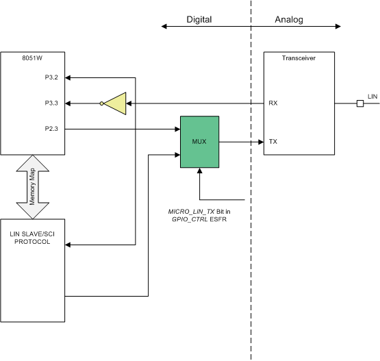 Figure 38. LIN Tx and Rx Pins Are Connected to 8051W Port Pins
The reason for routing the Rx pin to P3.2 and P3.3 is to allow the use of 8051W timer 1 to measure the durations of the LIN bus in the high or low state.
7.4 Device Functional Modes
7.4.1 Active Mode
The process of taking a measurement occurs when the device is in active mode. The low-side drivers, analog front-end, and digital data path are all active which allows for an ultrasonic signal to be transmitted and the reflected signal to be received and processed.
The maximum current (VREG not charging) in active mode is 15 mA.
To enter active mode, set the ACTIVE_EN bit in the PWR_MODE register to 1.
7.4.2 Quiet Mode
In quiet mode, the device waits for a command which is given through a digital interface (such as LIN, SCI, or UART). The LNA, ADC, digital data path, and low-side drivers are all off. The VREG regulator can be either enabled or disabled. If the VREG regulator is charging, the maximum current is increased by 100 mA.
The maximum current (VREG not charging) in quiet mode is 7.5 mA.
To enter quiet mode, set the ACTIVE_EN bit in the PWR_MODE register to 0.
7.4.3 RESET
The PGA450-Q1 can also be put into a RESET state where the microcontroller is not active. During this state, SPI is the only digital interface that can be used. The low-side drivers can still be triggered to begin an ultrasonic burst and the analog front-end and digital data path can still store the returned echo signal in the FIFO RAM. However, any processing of the FIFO RAM by the internal microprocessor to determine the location of an object does not occur. The FIFO RAM data can be read over SPI, allowing an external microprocessor to process the data.
While the microcontroller is active, the MICRO RESET test register is the only register accessible through SPI. The device must be put into the RESET state before sending additional SPI commands.
The maximum current (VREG not charging) in the RESET state is 15 mA.
To put the microcontroller in reset, write a 1 to bit 0 of the MICRO RESET (address 0x2F) test register. Transmit the TEST Write SPI command in the following order: 0x16, 0x2F, 0x01.
To bring the microcontroller out of reset, write a 0 to bit 0 of the MICRO RESET (address 0x2F) test register. Transmit the TEST Write SPI command in the following order: 0x16, 0x2F, 0x00.
NOTE
The MICRO RESET (0x2F) register is an internal test register, which is why the field is not listed in the SFR or ESFR register map.
7.5 Programming
7.5.1 SPI Interface
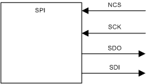 Figure 39. SPI Port in PGA450-Q1
The SPI block is used for communicating with the device during system development. The internal SPI acts as the slave in the communication of the device with an external SPI which is in master mode. To perform the communication, four external pins are necessary:
-
SDI: SPI slave-in master-out, serial-input pin
-
SDO: SPI slave-out master-in, serial-output pin (three-state output)
-
SCLK: SPI clock, which controls the communication
-
CS: Chip select
The output data on the SDO pin (for example, CheckByte and read data) changes on the rising edge of SCLK. The input data on SDI is latched on the falling edge of SCLK. The data received during a write access is written to memory on the system clock after the CS pin has gone high.
In the absence of active transmission, the master SPI resets the internal SPI with CS = high. MISO is in the high-impedance state during reset. Master and slave SPI transmit the MSB first.
NOTE
The PGA450-Q1 does not respond to SPI messages unless the 8051W microprocessor is in the reset state. The microprocessor can be put in the reset state by writing an appropriate value to the MICRO RESET test register. The MICRO RESET test register is the ONLY register that is accessible through the SPI when the 8051W processor is not in the reset state.
7.5.1.1 SPI Interface Protocol
The serial peripheral interface (SPI) uses a 1-byte command word and 2 or 3 additional bytes for the complete command.
Table 14 lists the SPI protocol.
Table 14. SPI Protocol Command Word
| BIT | FUNCTION |
|---|---|
| 15:13 | Always 3’b000 |
| 12:10 | Memory access control: 3’b001: OTP 3’b010: EXTERNAL RAM (FIFO, general-purpose) 3’b011: EEPROM 3’b100: IRAM 3’b101: TEST registers 3’b110: ESFR 3’b111: Development RAM |
| 9 | R/W Access: Write = 1 Read = 0 |
| 8 | Parity bit: Odd parity on bits 15:9 |
When accessing memory (IRAM, ESFR, OTP, EEPROM, FIFO RAM, DEV RAM), the internal registers bits 15:13 must all be zero. If these bits are not zero, the SPI command is rejected and the SPI failure bit is set (see CheckByte below).
7.5.1.2 Transfer Width
Table 15 lists how the SPI transfer width (number of bytes) varies depending on whether the SPI is a read or write to the IRAM, ESFR, EEPROM, OTP, or FIFO data access.
Table 15. SPI Protocol Transfer Widths
For a SPI transfer to the internal register file, the parity P depends on the address.
For SPI transfers to the memories (IRAM, ESFR, OTP), the read data is available on the next SPI transfer. That is, when reading from a memory location, the user must send a subsequent transfer to get the data back.
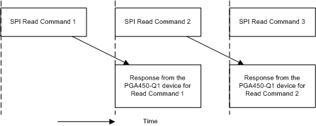 Figure 40. Response to SPI Read Commands Is Available When the Next Command Is Sent
7.5.1.3 CheckByte
On every SPI transfer, the PGA450-Q1 transmits a CheckByte which is in the 8 most significant bits of the transfer. For example, in a 16-bit transfer, the CheckByte is in bits 15:8 of the received data; similarly, for a 24 bit transfer the CheckByte is in bits 23:16 of the received data. The CheckByte can be used by the SPI master to detect SPI communication errors.
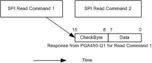 Figure 41. CheckByte Is Transmitted by PGA450-Q1 at the Beginning of Every Response
Table 16 lists the interpretation of each bit in the CheckByte transmitted by the PGA450-Q1.
For a successful SPI transfer, the CheckByte reads 8’h02. Bit 9 of the CheckByte is always set in order to assist debugging in the lab. If the SPI transfer failed for some reason, the most significant bit (15) of the CheckByte is set. The reason for the failure is then described in bits 14:11.
Table 16. SPI Protocol, CheckByte Field
| CheckByte BIT | ERROR | DESCRIPTION |
|---|---|---|
| 15 (or most significant bit) | SPI transfer failure | SPI transfer failure |
| 14 | Parity error | Parity error; command-byte parity incorrect |
| 13 | Illegal address | Illegal address; bits 15:13 and 12:10 cannot both be active |
| 12 | Illegal command | Illegal command; memory access bits 12:10 invalid |
| 11 | Wrong number of clocks | Wrong number clocks; must only receive 16, 24, or 32 clocks |
| 10:8 | Always 3’b010 | Always 3’b010 |
7.5.1.4 Examples
Table 17 lists a few examples of SPI transfer:
Table 17. SPI Protocol Examples
| COMMAND | SPI SLAVE TRANSFER |
|---|---|
| Read internal register 0 (revision id) | ({3’h0, 3’h0, 1’b0, 1’b1}, 8’hXX) |
| Write 0x80 to internal register 1 (MicroConfig) | ({3’h1, 3’h0, 1’b1, 1’b1}, 8’hC8) |
| Write 0x34 to internal RAM 0x7F | ({3’h0, 3’h4, 1’b1, 1’b1}, 8’h7F, 8’h34) |
| Read from ESFR 0xC0 | ({3’h0, 3’h6, 1’b0, 1’b1}, 8’hC0) |
| Write 0xD9 to OTP 0x1765 | ({3’h0, 3’h1, 1’b1, 1’b1}, 8’h17, 8’h65, 8’hD9) |
| Failed write 0xC8 to internal register 1 (bad parity) | ({3’h1, 3’h0, 1’b1, 1’b0}, 8’hC8) |
| Failed write 0xC8 to internal register 1 (illegal address) | ({3’h1, 3’h1, 1’b1, 1’b0}, 8’hC8) |
| Failed write 0x34 to memory (illegal command) | ({3’h0, 3’h7, 1’b1, 1’b1}, 8’h7F, 8’h34) |
7.5.2 Diagnostics
7.5.2.1 Power-Block Monitors
The following operating-condition monitors have been implemented on the PGA450-Q1 to ensure reliable and robust performance over the lifetime of the device.
- VPWR overvoltage (greater than 28 V nominal, 20-µs deglitch time)
- VPWR level is such that AVDD is undervoltage (less than 6 V nominal, 2-ms deglitch time)
- AVDD overcurrent (greater than 55 mA nominal, 2-ms deglitch time)
- RBIAS overcurrent (greater than 63 µA nominal, 2-ms deglitch time)
NOTE
Whenever these monitors sense a violation in the operating conditions, the
microprocessor is held in reset.
A corresponding fault flag is also set in the STATUS1 register.
The fault flags are cleared when the fault condition is removed or when the device is reset.
7.5.2.2 Low-Side Diagnostics
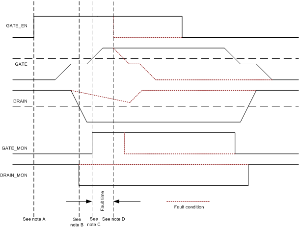
The PGA450-Q1 has diagnostics implemented on the LS driver to protect the LS FET from sinking excessive currents when it is enabled. A fault condition is sensed if both the Vgs voltage and the Vds voltage on the LS FET remain above 2.5 V for the duration of either 1 µs or 2 µs (selectable by setting the LS_FAULT_TIMER_SEL bit in the CONTROL_1 register) during a turnon event. If a fault is sensed, the LS FET is immediately turned off and a corresponding flag is set in the STATUS2 register. The fault is automatically cleared when the LS FET is commanded to turn on in the next cycle.
The LS diagnostics are turned off by default and can be enabled by setting the LS_FAULT_LOGIC_EN bit in the CONTROL_1 register.
Figure 42 shows the schematic of the low-side drive and Figure 43 shows the timing diagram of the low-side diagnostics.
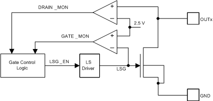 Figure 42. Low-Side Drive Schematic
7.5.2.3 Main Oscillator Watchdog
The PGA450-Q1 implements an internal free-running 500-kHz watchdog clock. This watchdog clock is used to monitor the internal 16-MHz main oscillator or the external crystal oscillator. When this frequency is outside this range, an internal reset is generated, which resets the entire digital core; this is equivalent to POR.
The main oscillator frequency fail limits have the following ranges as shown in Figure 44:
- If the main oscillator frequency is less than 5.4 MHz, the watchdog logic recognizes this as a low-frequency fail and resets the digital core.
- If the main oscillator frequency lies in the range: 5.4 MHz < Main OSC Freq < 14 MHz, there is a possibility that the watchdog recognizes this as a low-frequency fail and resets the core, but reset is not assured.
- If the main oscillator frequency lies in the range: 14 MHz < Main Osc Freq < 18 MHz, the main osc watchdog does NOT reset the core, as this is seen as the nominal frequency of operation.
- If the main oscillator frequency lies in the range 18 MHz < Main Osc Freq < 43 MHz, there is a possibility that the watchdog recognizes this as a high-frequency fail and resets the core, but reset is not assured.
- If the main oscillator frequency is greater than 43 MHz, the watchdog logic recognizes this as a high-frequency fail and resets the digital core.
 Figure 44. Main Oscillator Frequency and the Corresponding PGA450-Q1 Behavior
The main oscillator watchdog can be disabled using the OSC_WD_EN bit in the WD_EN register.
NOTE
A reset because of main oscillator watchdog failure causes an internal digital core reset. All ESFRs revert back to the reset sate.
7.5.2.4 Software Watchdog
The PGA450-Q1 implements a software watchdog. This watchdog must be serviced by software every 250 ms. If the software does not service the watchdog within 250 ms of the last service, then the transducer drive FETs are turned OFF and the 8051W core is reset.
The software services the watchdog using port pin P3.7 as shown in Figure 45. The software services the watchdog by toggling the state of P3.7.
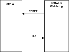 Figure 45. Connection Between the 8051W and the Software Watchdog
The software watchdog can be disabled using the SW_WD_EN bit in the WD_EN register. The following lists the behavior of this bit:
- The SW_WD_EN bit is in the disabled state after power-on reset (POR).
- If the 8051W is reset through the SPI, then SW_WD_EN is disabled.
- If SW_WD_EN is enabled and the 8051W is reset because the software watchdog has timed out, then SW_WD_EN remains enabled.
NOTE
A reset of the 8051W does not change the state of the ESFR registers. The ESFR registers continue to retain the state.
7.5.2.5 Internal ASIC TRIM Validity
The PGA450-Q1 has internal ASIC trim values. These trim values are used to fine-tune the operation of various blocks at TI manufacturing EOL.
The PGA450-Q1 checks the validity of these ASIC trim values after power up and before the 8051W reset is deasserted. If the internal trim values are not valid, the TRIM_FAIL bit in the STATUS1 register is set. The 8051W software can be used to check this bit after 8051W reset is deasserted and the software starts execution.
7.5.2.6 FIFO RAM and External SRAM MBIST
The PGA450-Q1 verifies the integrity of FIFO RAM and RAM in the external memory space (that is, all RAM in the external memory) with a RAM MBIST. The RAM MBIST begins immediately after POR is deasserted and takes approximately 5 ms. See Figure 8 for power-up waveforms. The 8051W reset is deasserted while MBIST is ongoing.
MBIST sets the MBIST_DONE flag in STATUS1 upon completion of MBIST. The MBIST_FLAG is set to 1 if RAM MBIST fails.
NOTE
The 8051W microprocessor should not enable the digital datapath, should not access the FIFO RAM, and should not access RAM in the external memory space until the RAM MBIST DONE flag is set.
7.5.2.7 Thermal Shutdown
The PGA450-Q1 also has an overtemperature protection feature implemented. An overtemperature violation causes a total shutdown of the part with the microprocessor held in reset. When the device cools down below the overtemperature threshold, the device initiates a power up again.
7.5.3 8051W Interrupts
The MCU 8051 provides the five standard 8051-compatible legacy interrupts, plus expansion capability for a further nine extended interrupts sourced from external user logic. The standard and extended interrupts each have separate enable-register bits associated with them, allowing software control. The interrupts can also have two levels of priority assigned to them. The interrupts are defined as follows:
-
Standard interrupts The five standard interrupts comprise two timer overflow interrupts, an interrupt associated with the built-in serial interface of the core, and two external interrupts (referred to as legacy external interrupts).
-
Timer-overflow interrupts The two timer-overflow interrupts, TF0 and TF1, are set whenever their respective timers timer 0 and timer 1, roll over to zero. The states of these interrupts are also stored in the TCON register. The TF0 and TF1 interrupts are automatically cleared by hardware on entry to the corresponding interrupt service routine.
NOTE
All events on NINT0 and NINT1, whether level-triggered or edge-triggered, are detected by sampling the relevant interrupt line on the rising edge of SCLK at the end of phase 1 of every machine cycle. Where NINT0/NINT1 is level-triggered, a response is made to the signal being sampled low and, to ensure detection, the external source must hold the line low until the resulting interrupt is generated. (It also must ensure that the request is de-activated before the end of the associated service routine.) Where NINT0 or NINT1 is edge-triggered, the response is made to a transition on the signal from high to low between successive samples. This means that, to ensure detection, NINT0 or NINT1 must have been high for at least two clocks before it goes low and then must be held low for at least two clocks after this transition.
-
Serial interrupt The serial interrupts source comprises the logical OR of the two serial interface status bits RI and TI in register SCON. These interrupts are set automatically on receipt or transmission of a data frame. These two bits are not cleared by hardware.
-
Legacy external interrupts The two legacy external interrupts, NINT0 and NINT1, are driven from inputs PORT3(2) and PORT3(3), respectively. These interrupts can be either edge- or level-sensitive, depending on settings within the TCON register. Two further TCON register bits, IE0 and IE1, act as interrupt flags. If the external interrupt is set to edge-triggered, the corresponding register bit IE0 or IE1 is set by a falling edge on NINT0 or NINT1 and cleared by hardware on entry to the corresponding interrupt service routine. If the interrupt is set to be level-sensitive, IE0or IE1 reflects the logic level on NINT0 or NINT1. The TCON register is described in the Timer and Counter Control Register (offset = 0x88) [reset = 0] section.
-
Extended interrupts Source and acknowledge signals are provided for a further nine interrupts. These interrupts are driven from external user logic, typically a user ESFR. The extended interrupts are input to the core on bits 5 to 13 of input bus XINTR_SRC, whereas acknowledge signals are output from the core on bits 5 to 13 of bus XINTR_ACK. Note: If the timers or the UART are omitted from the design, their corresponding interrupt inputs (plus those of the legacy external interrupts where the timers are omitted) are made available at the core periphery as XINTR_SRC[4:0], along with corresponding XINTR_ACK acknowledge signals, for use as additional extended interrupts.)
I
The extended-interrupt lines are sampled on the rising edge of PCLK at the beginning of phase 2 of the last cycle of the current instruction. To ensure detection, the external source must hold the XINTR_SRC line high until the resulting interrupt is generated and must also ensure that the request is deactivated before the end of the associated service routine.
I
Any edge-triggering that is required must be taken care of by individual peripherals.
NOTE
For additional information about these five standard interrupts, see the Intel 8-Bit Embedded Controller Handbook in the Hardware Description of the 8051, 8052 and 80C51.)
7.5.3.1 Interrupt Flag Clear
If the legacy external interrupts, NINT0 and NINT1, are edge-triggered, the interrupt flag is cleared on vectoring to the service routine. If these interrupts are level-triggered, the flag is controlled by the external signal. Timer and counter flags are cleared on vectoring to the interrupt service routine, but the serial interrupt flag is not affected by hardware. The serial interrupt flag should be cleared by software. Acknowledge signals are provided for clearing any registers used to source the nine additional interrupts.
7.5.3.2 Priority Levels and Interrupt Vectors
One of two priority levels can be selected for each interrupt. An interrupt of high priority may interrupt the service routine of a low-priority interrupt and, if two interrupts of different priority occur at the same time, the higher-level interrupt is serviced first. An interrupt cannot be interrupted by another interrupt of the same priority level. If two interrupts of the same priority level occur simultaneously, a polling sequence is observed as listed in Table 18:
When an interrupt is serviced, a long call instruction is executed to one of the following locations, according to the source of the interrupt as listed in Table 18.
Table 18. Interrupt Summary
| 8051W SOURCE | PGA450-Q1 SOURCE | VECTOR ADDRESS | POLLING SEQUENCE | FLAG | ENABLE | PRIORITY CONTROL |
|---|---|---|---|---|---|---|
| External interrupt 0 | LIN RX | 0x0003 | 1 (highest) | IE0 (TCON.1) | EX0 (IE.0) | PX0 (IP.0) |
| Timer and counter interrupt 0 | ← | 0x000B | 2 | TF0 (TCON.5) | ET0 (IE.1) | PT0 (IP.1) |
| External interrupt 1 | LIN ~RX | 0x0013 | 3 | IE1 (TCON.3) | EX1 (IE.2) | PX1 (IP.2) |
| Timer and counter interrupt 1 | ← | 0x001B | 4 | TF1 (TCON.7) | ET1 (IE.3) | PT1 (IP.3) |
| Serial port 0 | ← | 0x0023 | 5 | RI_0 (SCON0.0)TI_0 (SCON0.1) | ES0 (IE.4) | PS0 (IP.4) |
| External interrupt 5 | LIN PID received | 0x002B | 6 | — | EI5 (IE.5) | PI5 (IP.5) |
| External interrupt 6 | LIN/SCI DATA received | 0x0033 | 7 | — | EI6 (IE1.0) | PI6 (IP1.0) |
| External interrupt 7 | LIN/SCI data transmit complete | 0x003B | 8 | — | EI7 (IE1.1) | PI7 (IP1.1) |
| External interrupt 8 | LIN SYNC received | 0x0043 | 9 | — | EI8 (IE1.2) | PI8 (IP1.2) |
| External interrupt 9 | 0x004B | 10 | — | EI9 (IE1.3) | PI9 (IP1.3) | |
| External interrupt 10 | 0x0053 | 11 | — | EI10 (IE14) | P10 (IP1.4) | |
| External interrupt 11 | 0x005B | 12 | — | EI11 (IE1.5) | P11 (IP1.5) | |
| External interrupt 12 | 0x0063 | 13 | — | EI12 (IE1.6) | P12 (IP16) | |
| External interrupt 13 | 0x006B | 14 (Lowest) | — | EI13 (IE1.7) | P13 (IP.7) |
7.5.3.3 Interrupt Latency
The response time in a single interrupt system is between 3 and 9 machine cycles.
7.5.4 Instructions
The M8051 Warp instruction set is listed in Table 20. The following sections outline some of the supported features.
7.5.4.1 Addressing Modes
The M8051 Warp provides a variety of addressing modes, which are outlined as follows.
7.5.4.1.1 Direct Addressing
In direct addressing, the operand is specified by an 8-bit address field. Only internal data and SFRs can be accessed using this mode.
7.5.4.1.2 Indirect Addressing
In indirect addressing, the operand is specified by an address contained in a register. Two registers (R0 and R1) from the current bank or the data pointer can be used for addressing in this mode. Both internal and external data memory can be indirectly addressed.
7.5.4.1.3 Register Addressing
In register addressing, the operand is specified by the top 3 bits of the opcode, which selects one of the current bank of registers. Four banks of registers are available. The current bank is selected by bits 3 and 4 of the PSW.
7.5.4.1.4 Register Specific Addressing
Some instructions only operate on specific registers which is defined by the opcode. In particular, many accumulator operations and some stack pointer operations are defined in this manner.
7.5.4.1.5 Immediate Data
Instructions which use immediate data are 2 or 3 bytes long, and the immediate operand is stored in program memory as part of the instruction.
7.5.4.1.6 Indexed Addressing
Only program memory can be addressed using indexed addressing. This memory is intended for simple implementation of look-up tables. A 16-bit base register (either the PC or the DPTR) is combined with an offset stored in the accumulator to access data in program memory.
7.5.4.2 Arithmetic Instructions
The M8051 Warp implements ADD, ADDC (add with carry), SUBB (subtract with borrow), INC (increment), and DEC (decrement) functions, which can be used in most addressing modes. There are three accumulator-specific instructions, DA A (decimal adjust A), MUL AB (multiply A by B) and DIV AB (divide A by B).
7.5.4.3 Logical Instructions
The M8051 Warp implements ANL (AND logical), ORL (OR logical), and XRL (exclusive-OR logical) functions, which again can be used in most addressing modes. Seven accumulator-specific instructions are available, CLR A (clear A), CPL A (complement A), RL A (rotate left A), RLC A (rotate left through carry A), RR A (rotate right A), RRC A (rotate right through carry A), and SWAP A (swap nibbles of A).
7.5.4.4 Data Transfers
7.5.4.4.1 Internal Data Memory
Data can be moved from the accumulator to any internal data memory location, from any internal data memory location to the accumulator, and from any internal data memory location to any SFR or other internal data memory location.
7.5.4.4.2 External Data Memory
Data can be moved from the accumulator to or from an external memory location in one of two addressing modes. In 8-bit addressing mode, the external location is addressed by either R0 or R1; in 16-bit addressing mode, the location is addressed by the DPTR.
7.5.4.5 Jump Instructions
7.5.4.5.1 Unconditional Jumps
Four sorts of unconditional jump instructions are available. Short jumps (SJMP) are relative jumps (limited to –128 to 127 bytes), long jumps (LJMP) are absolute 16-bit jumps, and absolute jumps (AJMP) are absolute 11-bit jumps (that is, within a 2K byte memory page). The last type is an indexed jump, JMP @A+DPTR, which jumps to a location contained in the DPTR register, offset by a value stored in the accumulator.
7.5.4.5.2 Subroutine Calls and Returns
Only two sorts of subroutine call are available, ACALL and LCALL, which are absolute and long as previously described. Two return instructions are provided, RET and RETI. The latter is for interrupt service routines.
7.5.4.5.3 Conditional Jumps
Conditional jump instructions all use relative addressing and there fore are limited to the same –128- to 127-byte range as previously described.
7.5.4.6 Boolean Instructions
The bit-addressable registers in both the direct and SFR space can be manipulated using Boolean instructions. Logical functions are available which use the carry flag and an addressable bit as the operands and each addressable bit can be set, cleared, or tested in a jump instruction.
7.5.4.7 Flags
Table 19 lists the instructions that affect the flags generated by the ALU.
Table 19. Flag Summary
| INSTRUCTION | FLAG | INSTRUCTION | FLAG | ||||
|---|---|---|---|---|---|---|---|
| C | OV | AC | C | OV | AC | ||
| ADD | ? | ? | ? | CLRC | 0 | ||
| ADDC | ? | ? | ? | CPLC | ? | ||
| SUBB | ? | ? | ? | ANL C, bit | ? | ||
| MUL | 0 | ? | ANL C, /bit | ? | |||
| DIV | 0 | ? | ORL C, bit | ? | |||
| DA | ? | ORL C, /bit | ? | ||||
| RRC | ? | MOV C, bit | ? | ||||
| RLC | ? | CJNE | ? | ||||
| SETB C | 1 | ||||||
In Table 19, a 0 indicates that the flag is always cleared, a 1 indicates that the flag is always set, and a question mark (?) indicates that the state of the flag depends on the result of the operation. The flag specified as blank means that the state is unknown.
7.5.4.8 Instruction Table
Instructions are either 1, 2, or 3 bytes long as listed in the BYTES column of Table 20. Each instruction requires either 1, 2 or 4 machine cycles to execute as listed in Table 20. One machine cycle comprises 2 CCLK clock cycles.
Table 20. Instructions
In Table 20, an entry such as E8–EF indicates a continuous block of hex opcodes used for 8 different registers, the register numbers of which are defined by the lowest three bits of the corresponding code. Non-continuous blocks of codes, shown as 11→F1 (for example), are used for absolute jumps and calls, with the top 3 bits of the code being used to store the top three bits of the destination address.
The CJNE instructions use the abbreviation #d for immediate data; other instructions use #data.
7.5.5 8051W Port Usage
The 8051W has four I/O ports. lists the port usage in the PGA450-Q1 device.
Table 21. 8051W I/O Port Usage in PGA450-Q1
7.6 Register Maps
The memory block consists of SRAM, OTP, and EEPROM. The SRAM is used as storage for volatile software variables during program execution. The OTP consists of the program code and the EEPROM consists of calibrations.
Table 22. SFR Memory Map
| Address (hex) | Description | D6 | D5 | D4 | D3 | D2 | D1 | D0 | R/W | POWER ON Value |
|---|---|---|---|---|---|---|---|---|---|---|
| 80 | Port 0 (P0) | P0[6] | P0[5] | P0[4] | P0[3] | P0[2] | P0[1] | P0[0] | R/W | 0xFF |
| 81 | Stack Pointer | SP[6] | SP[5] | SP[4] | SP[3] | SP[2] | SP[1] | SP[0] | R/W | 0 |
| 82 | Data Pointer Low Byte | DPTR[6] | DPTR[5] | DPTR[4] | DPTR[3] | DPTR[2] | DPTR[1] | DPTR[0] | R/W | 0 |
| 83 | Data Pointer High Byte | DPTR[14] | DPTR[13] | DPTR[12] | DPTR[11] | DPTR[10] | DPTR[9] | DPTR[8] | R/W | 0 |
| 87 | Power control Register | GF1 | GF0 | PD | IDL | R/W | 0 | |||
| 88 | Timer / Counter Control | TR1 | TF0 | TR0 | IE1 | IT1 | IE0 | IT0 | R/W | 0 |
| 89 | Timer / Counter Mode | CNT1 | M1 (1) | M0 (1) | GATE0 | CNT0 | M1 (0) | M0 (0) | R/W | 0 |
| 8A | Timer / Counter Data (TL0) | TL0[6] | TL0[5] | TL0[4] | TL0[3] | TL0[2] | TL0[1] | TL0[0] | R/W | 0 |
| 8B | Timer / Counter Data (TL1) | TL1[6] | TL1[5] | TL1[4] | TL1[3] | TL1[2] | TL1[1] | TL1[0] | R/W | 0 |
| 8C | Timer / Counter Data (TH0) | TH0[6] | TH0[5] | TH0[4] | TH0[3] | TH0[2] | TH0[1] | TH0[0] | R/W | 0 |
| 8D | Timer / Counter Data (TH1) | TH1[6] | TH1[5] | TH1[4] | TH1[3] | TH1[2] | TH1[1] | TH1[0] | R/W | 0 |
| 90 | Port 1 (P1) | P1[6] | P1[5] | P1[4] | P1[3] | P1[2] | P1[1] | P1[0] | R/W | 0xFF |
| 98 | UART Control (SCON) | SM1 | SM2 | REN | TB8 | RB8 | TI | RI | R/W | 0 |
| 99 | UART Data (SBUF) | SBUF[6] | SBUF[5] | SBUF[4] | SBUF[3] | SBUF[2] | SBUF[1] | SBUF[0] | R/W | 0 |
| A0 | Port 2 (P2) | P2[6] | P2[5] | P2[4] | P2[3] | P2[2] | P2[1] | P2[0] | R/W | 0xFF |
| A8 | Interrupt Enable Register 0 | EI5 | ES | ET1 | EX1 | ET0 | EX0 | R/W | 0 | |
| B0 | Port 3 (P3) | P3[6] | P3[5] | P3[4] | P3[3] | P3[2] | P3[1] | P3[0] | R/W | 0xFF |
| B8 | Interrupt Priority Register 0 | PI5 | PS | PT1 | PX1 | PT0 | PX0 | R/W | 0 | |
| D0 | Program Status Word | AC | F0 | RS1 | RS0 | OV | F1 | P | R/W | 0 |
| E0 | Accumulator | ACC[6] | ACC[5] | ACC[4] | ACC[3] | ACC[2] | ACC[1] | ACC[0] | R/W | 0 |
| E8 | Interrupt Enable Register 1 | EI12 | EI11 | EI10 | EI9 | EI8 | EI7 | EI6 | R/W | 0 |
| F0 | Register (B) | B[6] | B[5] | B[4] | B[3] | B[2] | B[1] | B[0] | R/W | 0 |
| F8 | Interrupt Priority Register 1 | PI12 | PI11 | PI10 | PI9 | PI8 | PI7 | PI6 | R/W | 0 |
Table 23. ESFR Memory Map
| Address (hex) | D7 | D6 | D5 | D4 | D3 | D2 | D1 | D0 | R/W | Power Up | Description (Programmable Regs) |
|---|---|---|---|---|---|---|---|---|---|---|---|
| 92 | BPF_B1[15] | BPF_B114] | BPF_B1[13] | BPF_B1[12] | BPF_B1[11] | BPF_B1[10] | BPF_B1[9] | BPF_B1[8] | R/W | 0 | BPF_B1_MSB |
| 93 | BPF_B1[7] | BPF_B1[6] | BPF_B1[5] | BPF_B1[4] | BPF_B1[3] | BPF_B1[2] | BPF_B1[1] | BPF_B1[0] | R/W | 0 | BPF_B1_LSB |
| 94 | BPF_A2[15] | BPF_A2[14] | BPF_A2[13] | BPF_A2[12] | BPF_A2[11] | BPF_A2[10] | BPF_A2[9] | BPF_A2[8] | R/W | 0 | BPF_A2_MSB |
| 95 | BPF_A2[7] | BPF_A2[6] | BPF_A2[5] | BPF_A2[4] | BPF_A2[3] | BPF_A2[2] | BPF_A2[1] | BPF_A2[0] | R/W | 0 | BPF_A2_LSB |
| 96 | BPF_A3[15] | BPF_A3[14] | BPF_A3[13] | BPF_A3[12] | BPF_A3[11] | BPF_A3[10] | BPF_A3[9] | BPF_A3[8] | R/W | 0 | BPF_A3_MSB |
| 97 | BPF_A3[7] | BPF_A3[6] | BPF_A3[5] | BPF_A3[4] | BPF_A3[3] | BPF_A3[2] | BPF_A3[1] | BPF_A3[0] | R/W | 0 | BPF_A3_LSB |
| A1 | LPF_B1[14] | LPF_B1[13] | LPF_B1[12] | LPF_B1[11] | LPF_B1[10] | LPF_B1[9] | LPF_B1[8] | R/W | 0 | LPF_B1_MSB | |
| A2 | LPF_B1[7] | LPF_B1[6] | LPF_B1[5] | LPF_B1[4] | LPF_B1[3] | LPF_B1[2] | LPF_B1[1] | LPF_B1[0] | R/W | 0 | LPF_B1_LSB |
| A3 | LPF_A2[14] | LPF_A2[13] | LPF_A2[12] | LPF_A2[11] | LPF_A2[10] | LPF_A2[9] | LPF_A2[8] | R/W | 0 | LPF_A2_MSB | |
| A4 | LPF_A2[7] | LPF_A2[6] | LPF_A2[5] | LPF_A2[4] | LPF_A2[3] | LPF_A2[2] | LPF_A2[1] | LPF_A2[0] | R/W | 0 | LPF_A2_LSB |
| A5 | DS5 | DS4 | DS3 | DS2 | DS1 | DS0 | R/W | 0 | DOWNSAMPLE | ||
| A6 | ONA[10] | ONA[9] | ONA[8] | R/W | 0 | ONA_MSB | |||||
| A7 | ONA[7] | ONA[6] | ONA[5] | ONA[4] | ONA[3] | ONA[2] | ONA[1] | ONA[0] | R/W | 0 | ONA_LSB |
| A9 | OFFA[10] | OFFA[9] | OFFA[8] | R/W | 0 | OFFA_MSB | |||||
| AA | OFFA[7] | OFFA[6] | OFFA[5] | OFFA[4] | OFFA[3] | OFFA[2] | OFFA[1] | OFFA[0] | R/W | 0 | OFFA_LSB |
| AB | ONB[10] | ONB[9] | ONB[8] | R/W | 0 | ONB_MSB | |||||
| AC | ONB[7] | ONB[6] | ONB[5] | ONB[4] | ONB[3] | ONB[2] | ONB[1] | ONB[0] | R/W | 0 | ONB_LSB |
| AD | OFFB[10] | OFFB[9] | OFFB[8] | R/W | 0 | OFFB_MSB | |||||
| AE | OFFB[7] | OFFB[6] | OFFB[5] | OFFB[4] | OFFB[3] | OFFB[2] | OFFB[1] | OFFB[0] | R/W | 0 | OFFB_LSB |
| AF | PCA5 | PCA4 | PCA3 | PCA2 | PCA1 | PCA0 | R/W | 0 | PULSE_CNTA | ||
| B1 | PCB5 | PCB4 | PCB3 | PCB2 | PCB1 | PCB0 | R/W | 0 | PULSE_CNTB | ||
| B2 | DT7 | DT6 | DT5 | DT4 | DT3 | DT2 | DT1 | DT0 | R/W | 0 | DEADTIME |
| B3 | BMODE2 | BMODE1 | BMODE0 | R/W | 0 | BURST_MODE | |||||
| B4 | TS7 | TS6 | TS5 | TS4 | TS3 | TS2 | TS1 | TS0 | R | 0 | TEMP_SENS |
| B5 | SD7 | SD6 | SD5 | SD4 | SD3 | SD2 | SD1 | SD0 | R/W | 0 | SAT_DEGLITCH |
| B6 | ST7 | ST6 | ST5 | ST4 | ST3 | ST2 | ST1 | ST0 | R | 0 | SAT_TIME |
| B7 | LS_FAULT_LOGIC_EN | LS_FAULT_TIMER_SEL | LNA_GAIN1 | LNA_GAIN0 | SAT_SEL1 | SAT_SEL0 | R/W | 0 | CONTROL_1 | ||
| B9 | BT7 | BT6 | BT5 | BT4 | BT3 | BT2 | BT1 | BT0 | R/W | 0 | BLANKING_TIMER |
| BA | FRT[15] | FRT[14] | FRT[13] | FRT[12] | FRT[11] | FRT[10] | FRT[9] | FRT[8] | R | 0 | FRT_MSB |
| BB | FRT[7] | FRT[6] | FRT[5] | FRT[4] | FRT[3] | FRT[2] | FRT[1] | FRT[0] | R | 0 | FRT_LSB |
| BC | MICRO_LIN_TX | UARTTX_CONFIG | GPIO2_CONFIG2 | GPIO2_CONFIG1 | GPIO2_CONFIG0 | GPIO1_CONFIG2 | GPIO1_CONFIG1 | GPIO1_CONFIG0 | R/W | 0 | GPIO_CTRL |
| BD | CLK_SEL1 | CLK_SEL0 | R/W | 0 | CLK_SEL | ||||||
| BE | SW_WD_EN | OSC_WD_EN | R/W | 0 | WD_EN | ||||||
| BF | LIN_SCI | R/W | 0 | LIN_SCI | |||||||
| C0 | RELOAD | WRITE/EE_STATUS | R/W | 0 | EE_CTRL | ||||||
| C1 | TRIM_FAIL | MBIST_DONE | MBIST_FAIL | VPWR_OV | AVDD_UV | AVDD_OC | RBIAS_OC | R | N/A | STATUS1 | |
| C2 | WD_TO_OSC | LSB_FAULT | LSA_FAULT | WD_TO_SW | SAT_DONE | VREG_READY | R | N/A | STATUS2 | ||
| C3 | VREG_EN | ACTIVE_EN | R/W | 0 | PWR_MODE | ||||||
| C4 | FIFO_ADC | SCI_TX_EN | FIFO_PEAKDET | R/W | 0 | DP_SCI_CTRL | |||||
| C5 | NROLLOVER | FMODE1 | FMODE0 | R/W | 0 | FIFO_CTRL | |||||
| C8 | CAP_FR_TIMER | ECHO_EN | SAT_EN | BURST_B_EN | BURST_EN | R | N/A | EN_CTRL | |||
| C9 | RX_DATA1[7] | RX_DATA1[6] | RX_DATA1[5] | RX_DATA1[4] | RX_DATA1[3] | RX_DATA1[2] | RX_DATA1[1] | RX_DATA1[0] | R | N/A | RX_DATA1 |
| CA | RX_DATA2[7] | RX_DATA2[6] | RX_DATA2[5] | RX_DATA2[4] | RX_DATA2[3] | RX_DATA2[2] | RX_DATA2[1] | RX_DATA2[0] | R | N/A | RX_DATA2 |
| CB | RX_DATA3[7] | RX_DATA3[6] | RX_DATA3[5] | RX_DATA3[4] | RX_DATA3[3] | RX_DATA3[2] | RX_DATA3[1] | RX_DATA3[0] | R | N/A | RX_DATA3 |
| CC | RX_DATA4[7] | RX_DATA4[6] | RX_DATA4[5] | RX_DATA4[4] | RX_DATA4[3] | RX_DATA4[2] | RX_DATA4[1] | RX_DATA4[0] | R | N/A | RX_DATA4 |
| CD | RX_DATA5[7] | RX_DATA5[6] | RX_DATA5[5] | RX_DATA5[4] | RX_DATA5[3] | RX_DATA5[2] | RX_DATA5[1] | RX_DATA5[0] | R | N/A | RX_DATA5 |
| CE | RX_DATA6[7] | RX_DATA6[6] | RX_DATA6[5] | RX_DATA6[4] | RX_DATA6[3] | RX_DATA6[2] | RX_DATA6[1] | RX_DATA6[0] | R | N/A | RX_DATA6 |
| CF | RX_DATA7[7] | RX_DATA7[6] | RX_DATA7[5] | RX_DATA7[4] | RX_DATA7[3] | RX_DATA7[2] | RX_DATA7[1] | RX_DATA7[0] | R | N/A | RX_DATA7 |
| D1 | RX_DATA8[7] | RX_DATA8[6] | RX_DATA8[5] | RX_DATA8[4] | RX_DATA8[3] | RX_DATA8[2] | RX_DATA8[1] | RX_DATA8[0] | R | N/A | RX_DATA8 |
| D2 | PID7 | PID6 | PID5 | PID4 | PID3 | PID2 | PID1 | PID0 | R | N/A | LIN_PID |
| D3 | TX_DATA1[7] | TX_DATA1[6] | TX_DATA1[5] | TX_DATA1[4] | TX_DATA1[3] | TX_DATA1[2] | TX_DATA1[1] | TX_DATA1[0] | R/W | N/A | TX_DATA1 |
| D4 | TX_DATA2[7] | TX_DATA2[6] | TX_DATA2[5] | TX_DATA2[4] | TX_DATA2[3] | TX_DATA2[2] | TX_DATA2[1] | TX_DATA2[0] | R/W | N/A | TX_DATA2 |
| D5 | TX_DATA3[7] | TX_DATA3[6] | TX_DATA3[5] | TX_DATA3[4] | TX_DATA3[3] | TX_DATA3[2] | TX_DATA3[1] | TX_DATA3[0] | R/W | N/A | TX_DATA3 |
| D6 | TX_DATA4[7] | TX_DATA4[6] | TX_DATA4[5] | TX_DATA4[4] | TX_DATA4[3] | TX_DATA4[2] | TX_DATA4[1] | TX_DATA4[0] | R/W | N/A | TX_DATA4 |
| D7 | TX_DATA5[7] | TX_DATA5[6] | TX_DATA5[5] | TX_DATA5[4] | TX_DATA5[3] | TX_DATA5[2] | TX_DATA5[1] | TX_DATA5[0] | R/W | N/A | TX_DATA5 |
| D8 | TX_DATA6[7] | TX_DATA6[6] | TX_DATA6[5] | TX_DATA6[4] | TX_DATA6[3] | TX_DATA6[2] | TX_DATA6[1] | TX_DATA6[0] | R/W | N/A | TX_DATA6 |
| D9 | TX_DATA7[7] | TX_DATA7[6] | TX_DATA7[5] | TX_DATA7[4] | TX_DATA7[3] | TX_DATA7[2] | TX_DATA7[1] | TX_DATA7[0] | R/W | N/A | TX_DATA7 |
| DA | TX_DATA8[7] | TX_DATA8[6] | TX_DATA8[5] | TX_DATA8[4] | TX_DATA8[3] | TX_DATA8[2] | TX_DATA8[1] | TX_DATA8[0] | R/W | N/A | TX_DATA8 |
| DB | CNT3 | CNT2 | CNT1 | CNT0 | R/W | N/A | DATA_CNT | ||||
| DC | BIT_TOL | CS_METHOD | CLR_ERR | INTERBYTE_SPC | HOLD | IGNORE_DIAG | R/W | 0x40 | LIN_CFG | ||
| DD | RX_TX | R/W | N/A | LIN_CTRL | |||||||
| DE | BREAK_DEL | SYNC_LONG | SYNC_SHORT | STOP_BIT_SHORT | STOP_BIT_VAL | PARITY | CHECKSUM | R | N/A | LIN_STATUS | |
| DF | FIFO_PTR[9] | FIFO_PTR[8] | R/W | N/A | FIFO_POINTER_MSB | ||||||
| E1 | FIFO_PTR[7] | FIFO_PTR[6] | FIFO_PTR[5] | FIFO_PTR[4] | FIFO_PTR[3] | FIFO_PTR[2] | FIFO_PTR[1] | FIFO_PTR[0] | R | N/A | FIFO_POINTER_LSB |
| E2 | VREG_SEL3 | VREG_SEL2 | VREG_SEL1 | VREG_SEL0 | R/W | 0 | VREG_SEL | ||||
| E3 | SC[15] | SC[14] | SC[13] | SC[12] | SC[11] | SC[10] | SC[9] | SC[8] | R/W | 0 | SYNC_COUNT_MSB |
| E4 | SC[7] | SC[6] | SC[5] | SC[4] | SC[3] | SC[2] | SC[1] | SC[0] | R/W | 0 | SYNC_COUNT_LSB |
| E5 | TS_DAC_MODE | TS_DAC_EN | R/W | 0 | TEMP_DAC_CTRL | ||||||
| E6 | OVR | OS5 | OS4 | OS3 | OS2 | OS1 | OS0 | R/W | 0 | OSC_SYNC_CTRL | |
| E9 | AMUX3 | AMUX2 | AMUX1 | AMUX0 | R/W | 0 | ANALOG_MUX | ||||
| EA | DMUX4 | DMUX3 | DMUX2 | DMUX1 | DMUX0 | R/W | 0 | DIGITAL_MUX | |||
7.6.1 SFR Registers
7.6.1.1 I/O Ports (P0, P1, P2, P3) Registers
P0, P1, P2, and P3 are latches used to drive the 32 quasi-bidirectional I/O lines. On reset, these registers are all set to the value FF hex, which is input mode. Table 21 lists the port usage in the PGA450-Q1 device.
7.6.1.1.1 I/O Port 3 Register (offset = 0xB0) [reset = 0xFF]
Bit addressable
| 7 | 6 | 5 | 4 | 3 | 2 | 1 | 0 |
| P3[7] | P3[6] | P3[5] | P3[4] | P3[3] | P3[2] | P3[1] | P3[0] |
| R/W-1 | R/W-1 | R/W-1 | R/W-1 | R/W-1 | R/W-1 | W-1 | R-1 |
Table 24. P3 Register Field Descriptions
| Bit | Field | Type | Reset | Description |
|---|---|---|---|---|
| 7 | P3[7] | R/W | 1 | |
| 6 | P3[6] | R/W | 1 | |
| 5 | P3[5] | R/W | 1 | This bit has an alternate function as a T1 input |
| 4 | P3[4] | R/W | 1 | This bit has an alternate function as a T0 input |
| 3 | P3[3] | R/W | 1 | This bit has an alternate function as an NINT1 input |
| 2 | P3[2] | R/W | 1 | This bit has an alternate function as an NINT0 input |
| 1 | P3[1] | W | 1 | This bit has an alternate function as a TXD output. When functioning as a TXD output, this bit serial transmits data from the UART and transmit clock in UART mode 0. |
| 0 | P3[0] | R | 1 | This bit has an alternate function as a RXD input. When functioning as a RXD inupt, this bit serial receives data to the UART. |
7.6.1.1.2 I/O Port 2 Register (offset = 0xA0) [reset = 0xFF]
| 7 | 6 | 5 | 4 | 3 | 2 | 1 | 0 |
| P2[7] | P2[6] | P2[5] | P2[4] | P2[3] | P2[2] | P2[1] | P2[0] |
| R/W-1 | R/W-1 | R/W-1 | R/W-1 | R/W-1 | R/W-1 | R/W-1 | R/W-1 |
Table 25. P2 Register Field Descriptions
| Bit | Field | Type | Reset | Description |
|---|---|---|---|---|
| 7-0 | P2[7:0] | R/W | 1 |
7.6.1.1.3 I/O Port 1 Register (offset = 0x90) [reset = 0xFF]
| 7 | 6 | 5 | 4 | 3 | 2 | 1 | 0 |
| P1[7] | P1[6] | P1[5] | P1[4] | P1[3] | P1[2] | P1[1] | P1[0] |
| R/W-1 | R/W-1 | R/W-1 | R/W-1 | R/W-1 | R/W-1 | R/W-1 | R/W-1 |
Table 26. P1 Register Field Descriptions
| Bit | Field | Type | Reset | Description |
|---|---|---|---|---|
| 7-0 | P1[7:0] | R/W | 1 |
7.6.1.1.4 I/O Port 0 (P0) (offset = 0x80) [reset = 0xFF]
| 7 | 6 | 5 | 4 | 3 | 2 | 1 | 0 |
| P0[7] | P0[6] | P0[5] | P0[4] | P0[3] | P0[2] | P0[1] | P0[0] |
| R/W-1 | R/W-1 | R/W-1 | R/W-1 | R/W-1 | R/W-1 | R/W-1 | R/W-1 |
Table 27. P0 Register Field Descriptions
| Bit | Field | Type | Reset | Description |
|---|---|---|---|---|
| 7-0 | P0[7:0] | R/W | 1 |
7.6.1.2 Stack Pointer Register (offset = 0x81) [reset = 0]
Not bit-addressable
The SP register contains the stack pointer. The stack pointer is used to load the program counter into internal data memory during LCALL and ACALL instructions and is used to retrieve the program counter from memory during RET and RETI instructions. Data can also be saved on or retrieved from the stack using PUSH and POP instructions. Instructions that use the stack automatically pre-increment or post-decrement the stack pointer so that the stack pointer always points to the last byte written to the stack, that is, the top of the stack. On reset the stack pointer is set to 07h. The user must ensure that the location of the stack in internal data memory does not interfere with other data stored therein.
Another use of the scratchpad area is for the programmer stack. This area is selected using the stack pointer (SP, SFR 81h). Whenever a call or interrupt is invoked, the return address is placed on the stack. The stack is also available to the user for variables, and so forth, because the stack can be moved and there is no fixed location within the RAM designated as stack. The stack pointer defaults to 07h on reset, and the user can then move it as needed. The SP points to the last used value. Therefore, the next value placed on the stack is put at SP + 1. Each PUSH or CALL increments the SP by the appropriate value, and each POP or RET decrements it.
| 7 | 6 | 5 | 4 | 3 | 2 | 1 | 0 |
| SP[7] | SP[6] | SP[5] | SP[4] | SP[3] | SP[2] | SP[1] | SP[0] |
| R/W-0 | R/W-0 | R/W-0 | R/W-0 | R/W-0 | R/W-1 | R/W-1 | R/W-1 |
Table 28. SP Register Field Descriptions
| Bit | Field | Type | Reset | Description |
|---|---|---|---|---|
| 7-0 | SP[7:0] | R/W | 0 |
7.6.1.3 Data Pointer Registers
Not bit-addressable.
The data pointer (DPTR) is a 16-bit register that may be accessed through the two SFR locations, data-pointer high byte (DPH) and data-pointer low byte (DPL). Two true 16-bit operations are allowed on the data pointer, load immediate and increment. The data pointer is used to form 16-bit addresses for external data memory accesses (MOVX), for program byte moves (MOVC) and for indirect program jumps (JMP @A+DPTR). On reset, the data pointer is set to 0000h.
7.6.1.3.1 Data Pointer Register (offset = 0x82) [reset = 0]
This is the 8 LSB of the data pointer.
| 7 | 6 | 5 | 4 | 3 | 2 | 1 | 0 |
| DPTR[7] | DPTR[6] | DPTR[5] | DPTR[4] | DPTR[3] | DPTR[2] | DPTR[1] | DPTR[0] |
| R/W-0 | R/W-0 | R/W-0 | R/W-0 | R/W-0 | R/W-0 | R/W-0 | R/W-0 |
Table 29. DPL Register Field Descriptions
| Bit | Field | Type | Reset | Description |
|---|---|---|---|---|
| 7-0 | DPTR[7:0] | R/W | 0 |
7.6.1.3.2 Data Pointer Register (offset = 0x83) [reset = 0]
This is the 8 MSB of the data pointer.
| 7 | 6 | 5 | 4 | 3 | 2 | 1 | 0 |
| DPTR[15] | DPTR[14] | DPTR[13] | DPTR[12] | DPTR[11] | DPTR[10] | DPTR[9] | DPTR[8] |
| R/W-0 | R/W-0 | R/W-0 | R/W-0 | R/W-0 | R/W-0 | R/W-0 | R/W-0 |
Table 30. DPH Register Field Descriptions
| Bit | Field | Type | Reset | Description |
|---|---|---|---|---|
| 7-0 | DPTR[15:8] | R/W | 0 |
7.6.1.4 Power Control Register (offset = 0x87) [reset = 0]
Not bit-addressable.
| 7 | 6 | 5 | 4 | 3 | 2 | 1 | 0 |
| SMOD | — | GF[1:0] | PD | IDL | |||
| R/W-0 | R-0 | R/W-0 | R/W-0 | R/W-0 | |||
Table 31. PCON Register Field Descriptions
| Bit | Field | Type | Reset | Description |
|---|---|---|---|---|
| 7 | SMOD | R/W | 0 | Double baud rate bit. For use, see Table 40. |
| 6-4 | R | 0 | ||
| 3-2 | GF[1:0] | R/W | 0 | General-purpose flag bit |
| 1 | PD | R/W | 0 | Power-down bit. If 1, power-down mode is entered. |
| 0 | IDL | R/W | 0 | Idle bit. If 1, idle mode is entered. |
7.6.1.5 Timer and Counter Control Register (offset = 0x88) [reset = 0]
Bit Addressable.
Two 16-bit timer and counters are provided. The TCON and TMOD bits are used to set the mode of operation and to control the running and interrupt generation of the timer and counters. The timer andcounter values are stored in two pairs of 8-bit registers (TL0, TH0, TL1, and TH1).
| 7 | 6 | 5 | 4 | 3 | 2 | 1 | 0 |
| TF1 | TR1 | TF0 | TR0 | IE1 | IT1 | IE0 | IT0 |
| R/W-0 | R/W-0 | R/W-0 | R/W-0 | R/W-0 | R/W-0 | R/W-0 | R/W-0 |
Table 32. TCON Register Field Descriptions
| Bit | Field | Type | Reset | Description |
|---|---|---|---|---|
| 7 | TF1 | R/W | 0 | Timer 1 overflow flag. Set by hardware when timer and counter 1 overflows. Cleared by hardware when the processor calls the interrupt service routine. |
| 6 | TR1 | R/W | 0 | Timer 1 run control. If 1, timer runs; if 0, timer is halted. |
| 5 | TF0 | R/W | 0 | Timer 0 overflow flag. Set by hardware when timer and counter 0 overflows. Cleared by hardware when the processor calls the interrupt service routine. |
| 4 | TR0 | R/W | 0 | Timer 0 run control. If 1, timer runs; if 0, timer is halted. |
| 3 | IE1 | R/W | 0 | External Interrupt 1 edge flag. Set by hardware when an external interrupt 1 edge is detected. |
| 2 | IT1 | R/W | 0 | External Interrupt 1 control bit. If 1, external interrupt 1 is edge-triggered; if 0, external interrupt 1 is level-triggered. |
| 1 | IE0 | R/W | 0 | External Interrupt 0 edge flag. Set by hardware when an external interrupt 0 edge is detected. |
| 0 | IT0 | R/W | 0 | External Interrupt 0 control bit. If 1, external interrupt 0 is edge-triggered; if 0, external interrupt 0 is level-triggered |
7.6.1.6 Timer and Counter Mode Register (offset = 0x89) [reset = 0]
Not Bit Addressable.
| 7 | 6 | 5 | 4 | 3 | 2 | 1 | 0 |
| GATE1 | CNT1 | M1 (1) | M0 (1) | GATE0 | CNT0 | M1 (0) | M0 (0) |
| R/W-0 | R/W-0 | R/W-0 | R/W-0 | R/W-0 | R/W-0 | R/W-0 | R/W-0 |
Table 33. TMOD Register Field Descriptions
| Bit | Field | Type | Reset | Description |
|---|---|---|---|---|
| 7 | GATE1 | R/W | 0 | Timer 1 gate flag. When TR1 is set and GATE1= 1, timer and counter 1 only runs if the NINT1 pin is 1 (hardware control). When GATE1 = 0, timer and counter 1 only runs if TR1 = 1 (software control). |
| 6 | CNT1 | R/W | 0 | Timer and counter-1 selector. If 0, input is from the internal system clock; if 1, input is from the T1 pin. |
| 5 | M1 (1) | R/W | 0 | Timer 1 mode-control bit M1. |
| 4 | M0 (1) | R/W | 0 | Timer 1 mode-control bit M0. |
| 3 | GATE0 | R/W | 0 | Timer 0 gate flag. When TR0 is set and GATE0 = 1, timer and counter 0 only runs if NINT0 pin is 1 (hardware control). When GATE0 = 0, timer and counter 0 only runs if TR0 = 1 (software control). |
| 2 | CNT0 | R/W | 0 | Timer and counter 0 selector. If 0, input is from the internal system clock; if 1, input is from the T0 pin. |
| 1 | M1 (0) | R/W | 0 | Timer 0 mode-control bit M1 |
| 0 | M0 (0) | R/W | 0 | Timer 0 mode-control bit M0 |
Table 34. Timer Mode Control Bits
| M1 | M0 | Operating Mode |
|---|---|---|
| 0 | 0 | 13-bit timer and counter (M8048-compatible mode) |
| 0 | 1 | 16-bit timer and counter |
| 1 | 0 | 8-bit auto-reload timer and counter |
| 1 | 1 | Timer 0 is split into two halves. TL0 is an 8-bit timer and counter controlled by the standard timer 0 control bits. TH0 is an 8-bit timer and counter controlled by the standard timer 1 control bits. TH1 and TL1 are held (timer 1 is stopped). |
7.6.1.7 Timer and Counter Data Registers (TL0, TL1, TH0, TH1)
Not bit-addressable.
TL0 and TH0 are the low and high bytes, respectively, of timer and counter 0. TL1 and TH1 are the low and high bytes, respectively, of timer and counter 1. In mode 2, the TL register is an 8-bit counter, and TH stores the reload value. On reset, all timer and counter registers are 00h.
The timer-clock resolution is 8 MHz.
7.6.1.7.1 TL0 Register (offset = 0x8A) [reset = 0]
| 7 | 6 | 5 | 4 | 3 | 2 | 1 | 0 |
| TL0[7] | TL0[6] | TL0[5] | TL0[4] | TL0[3] | TL0[2] | TL0[1] | TL0[0] |
| R/W-0 | R/W-0 | R/W-0 | R/W-0 | R/W-0 | R/W-0 | R/W-0 | R/W-0 |
Table 35. TL0 Register Field Descriptions
| Bit | Field | Type | Reset | Description |
|---|---|---|---|---|
| 7-0 | TL0[7:0] | R/W | 0 |
7.6.1.7.2 TL1 Register (offset = 0x8B) [reset = 0]
| 7 | 6 | 5 | 4 | 3 | 2 | 1 | 0 |
| TL1[7] | TL1[6] | TL1[5] | TL1[4] | TL1[3] | TL1[2] | TL1[1] | TL1[0] |
| R/W-0 | R/W-0 | R/W-0 | R/W-0 | R/W-0 | R/W-0 | R/W-0 | R/W-0 |
Table 36. TL1 Register Field Descriptions
| Bit | Field | Type | Reset | Description |
|---|---|---|---|---|
| 7-0 | TL1[7:0] | R/W | 0 |
7.6.1.7.3 TH0 Register (offset = 0x8C) [reset = 0]
| 7 | 6 | 5 | 4 | 3 | 2 | 1 | 0 |
| TH0[7] | TH0[6] | TH0[5] | TH0[4] | TH0[3] | TH0[2] | TH0[1] | TH0[0] |
| R/W-0 | R/W-0 | R/W-0 | R/W-0 | R/W-0 | R/W-0 | R/W-0 | R/W-0 |
Table 37. TH0 Register Field Descriptions
| Bit | Field | Type | Reset | Description |
|---|---|---|---|---|
| 7-0 | TH0[7:0] | R/W | 0 |
7.6.1.7.4 TH1 Register (offset = 0x8D) [reset = 0]
| 7 | 6 | 5 | 4 | 3 | 2 | 1 | 0 |
| TH1[7] | TH1[6] | TH1[5] | TH1[4] | TH1[3] | TH1[2] | TH1[1] | TH1[0] |
| R/W-0 | R/W-0 | R/W-0 | R/W-0 | R/W-0 | R/W-0 | R/W-0 | R/W-0 |
Table 38. TH1 Register Field Descriptions
| Bit | Field | Type | Reset | Description |
|---|---|---|---|---|
| 7-0 | TH1[7:0] | R/W | 0 |
7.6.1.8 UART Control Register (offset = 0x98) [reset = 0]
Bit-addressable
The UART uses two SFRs: SCON and SBUF. SCON is the control register and SBUF is the data register. Data is written to SBUF for transmission and SBUF is read to obtain received data. The received-data and transmitted-data registers are independent.
SM2 enables multi-processor communication over a single serial line and modifies the foregoing as listed in Table 40. In modes 2 and 3, if SM2 is set then the receive interrupt is not generated if the received 9th data bit is 0. In mode 1, the receive interrupt is not generated unless a valid stop bit is received. In mode 0, SM2 should be 0.
| 7 | 6 | 5 | 4 | 3 | 2 | 1 | 0 |
| SM0 | SM1 | SM2 | REN | TB8 | RB8 | TI | RI |
| R/W-0 | R/W-0 | R/W-0 | R/W-0 | R/W-0 | R/W-0 | R/W-0 | R/W-0 |
Table 39. SCON Register Field Descriptions
| Bit | Field | Type | Reset | Description |
|---|---|---|---|---|
| 7 | SM0 | R/W | 0 | UART mode specifier |
| 6 | SM1 | R/W | 0 | UART mode specifier |
| 5 | SM2 | R/W | 0 | UART mode specifier |
| 4 | REN | R/W | 0 | If 1, enables reception; if 0, disables reception |
| 3 | TB8 | R/W | 0 | In modes 2 and 3, this is the 9th data bit sent. |
| 2 | RB8 | R/W | 0 | In modes 2 and 3, this is the 9th data bit received. In mode 1, if SM2 = 0, this is the stop bit received. In mode 0, this bit is not used. |
| 1 | TI | R/W | 0 | Transmit interrupt flag. This is set by hardware at the end of the 8th bit in mode 0, or at the beginning of the stop bit in other modes. Must be cleared by software. |
| 0 | RI | R/W | 0 | Receive interrupt flag. This is set by hardware at the end of the 8th bit in mode 0, or at the half-point of the stop bit in other modes. Must be cleared by software. |
Table 40. Mode Control Bit Operation(1)
| Mode | SM0 | SM1 | Operating Mode | Baud Rate |
|---|---|---|---|---|
| Mode 0 | 0 | 0 | Mode 0: 8-bit shift register. ftimer_clk /2 | Baud rate = ftimer_clk / 2 |
| Mode 1 | 0 | 1 | Mode 1: 8 bit UART. | Baud rate = (SMOD+1) × ftimer_clk / (32 × (256 – TH1)) |
| Mode 2 | 1 | 0 | Mode 2: 9 bit UART. | Baud rate = (SMOD + 1) × ftimer_clk / 64 |
| Mode 3 | 1 | 1 | Mode 3: 9 bit UART. | Baud rate = (SMOD + 1) × ftimer_clk / (32 × (256 – TH1)) |
7.6.1.9 UART Data Register (offset = 0x99) [reset = 0]
Not bit-addressable
This register is used for both transmit and receive data. Transmit data is written to this location and receive data is read from this location, but the two paths are independent.
| 7 | 6 | 5 | 4 | 3 | 2 | 1 | 0 |
| SBUF[7] | SBUF[6] | SBUF[5] | SBUF[4] | SBUF[3] | SBUF[2] | SBUF[1] | SBUF[0] |
| R/W-0 | R/W-0 | R/W-0 | R/W-0 | R/W-0 | R/W-0 | R/W-0 | R/W-0 |
Table 41. SBUF Register Field Descriptions
| Bit | Field | Type | Reset | Description |
|---|---|---|---|---|
| 7-0 | SBUF[7:0] | R/W | 0 |
7.6.1.10 Interrupt Enable Register 0 (offset = 0xA8) [reset = 0]
Bit-addressable.
The two interrupt enable registers (IE0 and IE1) control the 14 available interrupts. Five of these interrupts are standard 8051-compatible legacy interrupts. The other nine are specific to the PGA450-Q1 device. More information on interrupts can be found in the 8051W Interrupts section.
For each bit in this register, a 1 enables the corresponding interrupt, and a 0 disables it.
| 7 | 6 | 5 | 4 | 3 | 2 | 1 | 0 |
| EA | — | EI5 | ES | ET1 | EX1 | ET0 | EX0 |
| R/W-0 | R-0 | R/W-0 | R/W-0 | R/W-0 | R/W-0 | R/W-0 | R/W-0 |
Table 42. IE0 Register Field Descriptions
| Bit | Field | Type | Reset | Description |
|---|---|---|---|---|
| 7 | EA | R/W | 0 | Enable or disable all interrupt bits. |
| 6 | R | 0 | ||
| 5 | EI5 | R/W | 0 | Enable external Interrupt 5, the LIN PID received interrupt. |
| 4 | ES | R/W | 0 | Enable serial port interrupt. |
| 3 | ET1 | R/W | 0 | Enable timer 1 overflow interrupt. |
| 2 | EX1 | R/W | 0 | Enable external interrupt 1, the NINT1 interrupt. |
| 1 | ET0 | R/W | 0 | Enable timer 0 overflow interrupt. |
| 0 | EX0 | R/W | 0 | Enable external interrupt 0, the NINT0 interrupt. |
7.6.1.11 Interrupt Enable Register 1 (offset = 0xE8) [reset = 0]
Bit-addressable.
See the 8051W Interrupts section for more information on available interrupts.
For each bit in this register, a 1 enables the corresponding interrupt, and a 0 disables it.
| 7 | 6 | 5 | 4 | 3 | 2 | 1 | 0 |
| EI13 | EI12 | EI11 | EI10 | EI9 | EI8 | EI7 | EI6 |
| R/W-0 | R/W-0 | R/W-0 | R/W-0 | R/W-0 | R/W-0 | R/W-0 | R/W-0 |
Table 43. IE1 Register Field Descriptions
| Bit | Field | Type | Reset | Description |
|---|---|---|---|---|
| 7 | EI13 | R/W | 0 | Enable external interrupt 13. |
| 6 | EI12 | R/W | 0 | Enable external interrupt 12. |
| 5 | EI11 | R/W | 0 | Enable external interrupt 11. |
| 4 | EI10 | R/W | 0 | Enable external interrupt 10. |
| 3 | EI9 | R/W | 0 | Enable external interrupt 9. |
| 2 | EI8 | R/W | 0 | Enable external interrupt 8, the LIN SYNC received interrupt. |
| 1 | EI7 | R/W | 0 | Enable external interrupt 7, the LIN/SCI data transmit complete interrupt. |
| 0 | EI6 | R/W | 0 | Enable external interrupt 6, the LIN/SCI data received interrupt. |
7.6.1.12 Interrupt Priority Register 0 (offset = 0xB8) [reset = 0]
Bit-addressable.
For each bit in this register, a setting of 1 selects high priority for the corresponding interrupt, and a setting of 0 selects low priority. While an interrupt is being serviced, it may only be interrupted by a higher priority interrupt. See the 8051W Interrupts section for more information on available interrupts.
| 7 | 6 | 5 | 4 | 3 | 2 | 1 | 0 |
| — | PI5 | PS | PT1 | PX1 | PT0 | PX0 | |
| R-0 | R/W-0 | R/W-0 | R/W-0 | R/W-0 | R/W-0 | R/W-0 | |
Table 44. IP0 Register Field Descriptions
| Bit | Field | Type | Reset | Description |
|---|---|---|---|---|
| 7-6 | R | 0 | ||
| 5 | PI5 | R/W | 0 | Select priority for external interrupt 5, the LIN PID received interrupt. |
| 4 | PS | R/W | 0 | Select priority for serial port interrupt. |
| 3 | PT1 | R/W | 0 | Select priority for timer 1 overflow interrupt. |
| 2 | PX1 | R/W | 0 | Select priority for external interrupt 1, the NINT1 interrupt. |
| 1 | PT0 | R/W | 0 | Select priority for timer 0 overflow interrupt. |
| 0 | PX0 | R/W | 0 | Select priority for external interrupt 0, the NINT0 interrupt. |
7.6.1.13 Interrupt Priority Register 1 (offset = 0xF8) [reset = 0]
Bit-addressable
For each bit in this register, a setting of 1 selects high priority for the corresponding interrupt, and a setting 0 selects low priority. While an interrupt is being serviced, it may only be interrupted by a higher priority interrupt. See the 8051W Interrupts section for more information on available interrupts.
| 7 | 6 | 5 | 4 | 3 | 2 | 1 | 0 |
| PI13 | PI12 | PI11 | PI10 | PI9 | PI8 | PI7 | PI6 |
| R/W-0 | R/W-0 | R/W-0 | R/W-0 | R/W-0 | R/W-0 | R/W-0 | R/W-0 |
Table 45. IP1 Register Field Descriptions
| Bit | Field | Type | Reset | Description |
|---|---|---|---|---|
| 7 | PI13 | R/W | 0 | Select priority for external interrupt 13. |
| 6 | PI12 | R/W | 0 | Select priority for external interrupt 12. |
| 5 | PI11 | R/W | 0 | Select priority for external interrupt 11. |
| 4 | PI10 | R/W | 0 | Select priority for external interrupt 10. |
| 3 | PI9 | R/W | 0 | Select priority for external interrupt 9. |
| 2 | PI8 | R/W | 0 | Select priority for external interrupt 8, the LIN SYNC received interrupt. |
| 1 | PI7 | R/W | 0 | Select priority for external interrupt 7, the LIN/SCI data transmit complete interrupt. |
| 0 | PI6 | R/W | 0 | Select priority for external interrupt 6, the LIN/SCI data received interrupt. |
7.6.1.14 Program Status Word Register (offset = 0xD0) [reset = 0]
Bit-addressable
This register contains status information resulting from CPU and ALU operation.
| 7 | 6 | 5 | 4 | 3 | 2 | 1 | 0 |
| CY | AC | F0 | RS1 | RS0 | OV | F1 | P |
| R/W-0 | R/W-0 | R/W-0 | R/W-0 | R/W-0 | R/W-0 | R/W-0 | R/W-0 |
Table 46. PSW Register Field Descriptions
| Bit | Field | Type | Reset | Description |
|---|---|---|---|---|
| 7 | CY | R/W | 0 | ALU carry flag |
| 6 | AC | R/W | 0 | ALU auxiliary carry flag |
| 5 | F0 | R/W | 0 | General-purpose user-definable flag |
| 4 | RS1 | R/W | 0 | Register bank-select bit 1 |
| 3 | RS0 | R/W | 0 | Register bank-select bit 0 |
| 2 | OV | R/W | 0 | ALU overflow flag |
| 1 | F1 | R/W | 0 | User-definable flag |
| 0 | P | R/W | 0 | Parity flag. Set each instruction cycle to indicate odd or even parity in the accumulator. |
Table 47. Register Bank-Select Bit Operation
| RS1 | RS0 | Register Bank Select |
|---|---|---|
| 0 | 0 | RB0: registers from 0x00–0x07 |
| 0 | 1 | RB1: Registers from 0x08–0x0F |
| 1 | 0 | RB2: Registers from 0x10–0x17 |
| 1 | 1 | RB3: Registers from 0x18–0x1F |
7.6.1.15 Accumulator Register (offset = 0xE0) [reset = 0]
Bit-addressable
This register provides one of the operands for most ALU operations which is denoted as A in the instruction table.
| 7 | 6 | 5 | 4 | 3 | 2 | 1 | 0 |
| ACC[7] | ACC[6] | ACC[5] | ACC[4] | ACC[3] | ACC[2] | ACC[1] | ACC[0] |
| R/W-0 | R/W-0 | R/W-0 | R/W-0 | R/W-0 | R/W-0 | R/W-0 | R/W-0 |
Table 48. ACC Register Field Descriptions
| Bit | Field | Type | Reset | Description |
|---|---|---|---|---|
| 7-0 | ACC[7:0] | R/W | 0 |
7.6.1.16 B Register (offset = 0xF0) [reset = 0]
Bit-addressable
This register provides the second operand for multiply or divide instructions which is denoted as B in the instruction table. Otherwise, the register may be used as a scratch pad register.
| 7 | 6 | 5 | 4 | 3 | 2 | 1 | 0 |
| B[7] | B[6] | B[5] | B[4] | B[3] | B[2] | B[1] | B[0] |
| R/W-0 | R/W-0 | R/W-0 | R/W-0 | R/W-0 | R/W-0 | R/W-0 | R/W-0 |
Table 49. B Register Field Descriptions
| Bit | Field | Type | Reset | Description |
|---|---|---|---|---|
| 7-0 | B[7:0] | R/W | 0 |
7.6.2 ESFR Registers
7.6.2.1 Bandpass Filter Coefficient B1 (BPF_B1) Register
Not bit-addressable.
These registers store the B1 coefficient value for the 2nd order Butterworth bandpass IIR filter. The B1 coefficient helps set the bandwidth of the bandpass filter, which can be programmed from 4 kHz to 7kHz. The specific values to program into these registers for each bandwidth are listed in Table 7.
7.6.2.1.1 Bandpass Filter B1 MSB Register (offset = 0x92) [reset = 0]
| 7 | 6 | 5 | 4 | 3 | 2 | 1 | 0 |
| BPF_B1[15] | BPF_B1[14] | BPF_B1[13] | BPF_B1[12] | BPF_B1[11] | BPF_B1[10] | BPF_B1[9] | BPF_B1[8] |
| R/W-0 | R/W-0 | R/W-0 | R/W-0 | R/W-0 | R/W-0 | R/W-0 | R/W-0 |
Table 50. BPF_B1_MSB Register Field Descriptions
| Bit | Field | Type | Reset | Description |
|---|---|---|---|---|
| 7-0 | BPF_B1[15:8] | R/W | 0 |
7.6.2.1.2 Bandpass Filter B1 LSB Register (offset = 0x93) [reset = 0]
| 7 | 6 | 5 | 4 | 3 | 2 | 1 | 0 |
| BPF_B1[7] | BPF_B1[6] | BPF_B1[5] | BPF_B1[4] | BPF_B1[3] | BPF_B1[2] | BPF_B1[1] | BPF_B1[0] |
| R/W-0 | R/W-0 | R/W-0 | R/W-0 | R/W-0 | R/W-0 | R/W-0 | R/W-0 |
Table 51. BPF_B1_LSB Register Field Descriptions
| Bit | Field | Type | Reset | Description |
|---|---|---|---|---|
| 7-0 | BPF_B1[7:0] | R/W | 0 |
7.6.2.2 Bandpass Filter Coefficient A2 (BPF_A2) Registers
Not bit-addressable
These registers store the A2 coefficient value for the 2nd order Butterworth bandpass IIR filter. The A2 coefficient helps set the center frequency of the bandpass filter, which can be programmed from 40 kHz to 70 kHz. The specific values to program into these registers for each center frequency are listed in Table 8.
7.6.2.2.1 Bandpass Filter Coefficient A2 MSB Register (offset = 0x94) [reset = 0]
| 7 | 6 | 5 | 4 | 3 | 2 | 1 | 0 |
| BPF_A2[15] | BPF_A2[14] | BPF_A2[13] | BPF_A2[12] | BPF_A2[11] | BPF_A2[10] | BPF_A2[9] | BPF_A2[8] |
| R/W-0 | R/W-0 | R/W-0 | R/W-0 | R/W-0 | R/W-0 | R/W-0 | R/W-0 |
Table 52. BPF_A2_MSB Register Field Descriptions
| Bit | Field | Type | Reset | Description |
|---|---|---|---|---|
| 7-0 | BPF_A2[15:8] | R/W | 0 |
7.6.2.2.2 Bandpass Filter Coefficient A2 LSB Register (offset = 0x95) [reset = 0]
| 7 | 6 | 5 | 4 | 3 | 2 | 1 | 0 |
| BPF_A2[7] | BPF_A2[6] | BPF_A2[5] | BPF_A2[4] | BPF_A2[3] | BPF_A2[2] | BPF_A2[1] | BPF_A2[0] |
| R/W-0 | R/W-0 | R/W-0 | R/W-0 | R/W-0 | R/W-0 | R/W-0 | R/W-0 |
Table 53. BPF_A2_LSB Register Field Descriptions
| Bit | Field | Type | Reset | Description |
|---|---|---|---|---|
| 7-0 | BPF_A2[7:0] | R/W | 0 |
7.6.2.3 Band-Pass Filter Coefficient A3 (BPF_A3) Register
Not bit-addressable
These registers store the A3 coefficient value for the 2nd order Butterworth bandpass IIR filter. The A3 coefficient helps set the bandwidth of the bandpass filter, which can be programmed from 4 kHz to 7kHz. The specific values to program into these registers for each bandwidth are listed in Table 7.
7.6.2.3.1 Band-Pass Filter Coefficient A3 MSB Register (offset = 0x96) [reset = 0]
| 7 | 6 | 5 | 4 | 3 | 2 | 1 | 0 |
| BPF_A3[15] | BPF_A3[14] | BPF_A3[13] | BPF_A3[12] | BPF_A3[11] | BPF_A3[10] | BPF_A3[9] | BPF_A3[8] |
| R/W-0 | R/W-0 | R/W-0 | R/W-0 | R/W-0 | R/W-0 | R/W-0 | R/W-0 |
Table 54. BPF_A3_MSB Register Field Descriptions
| Bit | Field | Type | Reset | Description |
|---|---|---|---|---|
| 7-0 | BPF_A3[15:8] | R/W | 0 |
7.6.2.3.2 Band-Pass Filter Coefficient A3 LSB Register (offset = 0x97) [reset = 0]
| 7 | 6 | 5 | 4 | 3 | 2 | 1 | 0 |
| BPF_A3[7] | BPF_A3[6] | BPF_A3[5] | BPF_A3[4] | BPF_A3[3] | BPF_A3[2] | BPF_A3[1] | BPF_A3[0] |
| R/W-0 | R/W-0 | R/W-0 | R/W-0 | R/W-0 | R/W-0 | R/W-0 | R/W-0 |
Table 55. BPF_A3_LSB Register Field Descriptions
| Bit | Field | Type | Reset | Description |
|---|---|---|---|---|
| 7-0 | BPF_A3[7:0] | R/W | 0 |
7.6.2.4 Low-Pass Filter Coefficient B1 (LPF_B1) Registers
Not bit-addressable
These registers store the B1 coefficient value for the 1st order Butterworth low-pass IIR filter. The low-pass filter can be programmed with a cut-off frequency from 0.5 to 4 kHz. The specific values to program into these registers for each cut-off frequency are listed in Table 9.
7.6.2.4.1 Low-Pass Filter Coefficient B1 MSB Register (offset = 0xA1) [reset = 0]
| 7 | 6 | 5 | 4 | 3 | 2 | 1 | 0 |
| — | LPF_B1[14] | LPF_B1[13] | LPF_B1[12] | LPF_B1[11] | LPF_B1[10] | LPF_B1[9] | LPF_B1[8] |
| R/W-0 | R/W-0 | R/W-0 | R/W-0 | R/W-0 | R/W-0 | R/W-0 | R/W-0 |
Table 56. LPF_B1_MSB Register Field Descriptions
| Bit | Field | Type | Reset | Description |
|---|---|---|---|---|
| 7 | R/W | 0 | ||
| 6-0 | LPF_B1[14:8] | R/W | 0 |
7.6.2.4.2 Low-Pass Filter Coefficient B1 LSB Register (offset = 0xA2) [reset = 0]
| 7 | 6 | 5 | 4 | 3 | 2 | 1 | 0 |
| LPF_B1[7] | LPF_B1[6] | LPF_B1[5] | LPF_B1[4] | LPF_B1[3] | LPF_B1[2] | LPF_B1[1] | LPF_B1[0] |
| R/W-0 | R/W-0 | R/W-0 | R/W-0 | R/W-0 | R/W-0 | R/W-0 | R/W-0 |
Table 57. LPF_B1_LSB Register Field Descriptions
| Bit | Field | Type | Reset | Description |
|---|---|---|---|---|
| 7-0 | LPF_B1[7:0] | R/W | 0 |
7.6.2.5 Low-Pass Filter Coefficient A2 (LPF_A2) Registers
Not bit-addressable
These registers store the A2 coefficient value for the 1st order Butterworth low-pass IIR filter. The low-pass filter can be programmed with a cut-off frequency from 0.5 to 4 kHz. The specific values to program into these registers for each cut-off frequency are listed in Table 9.
7.6.2.5.1 Low-Pass Filter Coefficient A2 MSB Register (offset = 0xA3) [reset = 0]
| 7 | 6 | 5 | 4 | 3 | 2 | 1 | 0 |
| — | LPF_A2[14] | LPF_A2[13] | LPF_A2[12] | LPF_A2[11] | LPF_A2[10] | LPF_A2[9] | LPF_A2[8] |
| R/W-0 | R/W-0 | R/W-0 | R/W-0 | R/W-0 | R/W-0 | R/W-0 | R/W-0 |
Table 58. LPF_A2_MSB Register Field Descriptions
| Bit | Field | Type | Reset | Description |
|---|---|---|---|---|
| 7 | R/W | 0 | ||
| 6-0 | LPF_A2[14:8] | R/W | 0 |
7.6.2.5.2 Low-Pass Filter Coefficient A2 LSB Register (offset = 0xA4) [reset = 0]
| 7 | 6 | 5 | 4 | 3 | 2 | 1 | 0 |
| LPF_A2[7] | LPF_A2[6] | LPF_A2[5] | LPF_A2[4] | LPF_A2[3] | LPF_A2[2] | LPF_A2[1] | LPF_A2[0] |
| R/W-0 | R/W-0 | R/W-0 | R/W-0 | R/W-0 | R/W-0 | R/W-0 | R/W-0 |
Table 59. LPF_A2_LSB Register Field Descriptions
| Bit | Field | Type | Reset | Description |
|---|---|---|---|---|
| 7-0 | LPF_A2[7:0] | R/W | 0 |
7.6.2.6 Downsample Register (offset = 0xA5) [reset = 0]
Not bit-addressable.
This register sets the downsample rate in the datapath. If the low-pass filter is needed, then the downsampling rate must be set between 25 and 50. If the low-pass filter is not needed, then the DOWNSAMPLE register must be set between 1 and 63.
| 7 | 6 | 5 | 4 | 3 | 2 | 1 | 0 |
| – | DS5 | DS4 | DS3 | DS2 | DS1 | DS0 | |
| R/W-0 | R/W-0 | R/W-0 | R/W-0 | R/W-0 | R/W-0 | R/W-0 | |
Table 60. DOWNSAMPLE Register Field Descriptions
| Bit | Field | Type | Reset | Description |
|---|---|---|---|---|
| 7-6 | R/W | 0 | ||
| 5 | DS5 | R/W | 0 | |
| 4 | DS4 | R/W | 0 | |
| 3 | DS3 | R/W | 0 | |
| 2 | DS2 | R/W | 0 | |
| 1 | DS1 | R/W | 0 | |
| 0 | DS0 | R/W | 0 |
7.6.2.7 BURST ON A Duration (ON_A) Registers
Not bit-addressable
The ON_A register sets the duration that OUTA is held high during one burst. To generate a square wave of a particular frequency (fburst):
The resolution is 62.5 ns.
7.6.2.7.1 BURST ON A Duration MSB Register (offset = 0xA6) [reset = 0]
| 7 | 6 | 5 | 4 | 3 | 2 | 1 | 0 |
| — | ONA[10] | ONA[9] | ONA[8] | ||||
| R/W-0 | R/W-0 | R/W-0 | R/W-0 | ||||
Table 61. ONA_MSB Register Field Descriptions
| Bit | Field | Type | Reset | Description |
|---|---|---|---|---|
| 7-3 | R/W | 0 | ||
| 2-0 | ONA[10:8] | R/W | 0 |
7.6.2.7.2 BURST ON A Duration LSB Register (offset = 0xA7) [reset = 0]
| 7 | 6 | 5 | 4 | 3 | 2 | 1 | 0 |
| ONA[7] | ONA[6] | ONA[5] | ONA[4] | ONA[3] | ONA[2] | ONA[1] | ONA[0] |
| R/W-0 | R/W-0 | R/W-0 | R/W-0 | R/W-0 | R/W-0 | R/W-0 | R/W-0 |
Table 62. ONA_LSB Register Field Descriptions
| Bit | Field | Type | Reset | Description |
|---|---|---|---|---|
| 7-0 | ONA[7:0] | R/W | 0 |
7.6.2.8 BURST OFFA Duration (OFF_A) Register
Not bit-addressable
The OFF_A register sets the duration that OUTA is held low during one bust. To generate a square wave of a particular frequency, set OFF_A = ON_A. The resolution is 62.5 ns.
7.6.2.8.1 BURST OFFA Duration MSB Register (offset = 0xA9) [reset = 0]
| 7 | 6 | 5 | 4 | 3 | 2 | 1 | 0 |
| — | OFFA[10] | OFFA[9] | OFFA[8] | ||||
| R/W-0 | R/W-0 | R/W-0 | R/W-0 | ||||
Table 63. OFFA_MSB Register Field Descriptions
| Bit | Field | Type | Reset | Description |
|---|---|---|---|---|
| 7-3 | R/W | 0 | ||
| 2-0 | OFFA[10:8] | R/W | 0 |
7.6.2.8.2 BURST OFFA Duration LSB Register (offset = 0xAA) [reset = 0]
| 7 | 6 | 5 | 4 | 3 | 2 | 1 | 0 |
| OFFA[7] | OFFA[6] | OFFA[5] | OFFA[4] | OFFA[3] | OFFA[2] | OFFA[1] | OFFA[0] |
| R/W-0 | R/W-0 | R/W-0 | R/W-0 | R/W-0 | R/W-0 | R/W-0 | R/W-0 |
Table 64. OFFA_LSB Register Field Descriptions
| Bit | Field | Type | Reset | Description |
|---|---|---|---|---|
| 7-0 | OFFA[7:0] | R/W | 0 |
7.6.2.9 BURST ON B Duration (ON_B) Registers
Not bit-addressable
The ON_B register sets the duration that OUTB is held high during one burst. To generate a square wave of a particular frequency (fburst):
The resolution is 62.5 ns.
7.6.2.9.1 BURST ON B Duration MSB Register (offset = 0xAB) [reset = 0]
| 7 | 6 | 5 | 4 | 3 | 2 | 1 | 0 |
| — | ONB[10] | ONB[9] | ONB[8] | ||||
| R/W-0 | R/W-0 | R/W-0 | R/W-0 | ||||
Table 65. ONB_MSB Register Field Descriptions
| Bit | Field | Type | Reset | Description |
|---|---|---|---|---|
| 7-3 | R/W | 0 | ||
| 2-0 | ONB[10:8] | R/W | 0 |
7.6.2.9.2 BURST ON B Duration LSB Register (offset = 0xAC) [reset = 0]
| 7 | 6 | 5 | 4 | 3 | 2 | 1 | 0 |
| ONB[7] | ONB[6] | ONB[5] | ONB[4] | ONB[3] | ONB[2] | ONB[1] | ONB[0] |
| R/W-0 | R/W-0 | R/W-0 | R/W-0 | R/W-0 | R/W-0 | R/W-0 | R/W-0 |
Table 66. ONB_LSB Register Field Descriptions
| Bit | Field | Type | Reset | Description |
|---|---|---|---|---|
| 7-0 | ONB[7:0] | R/W | 0 |
7.6.2.10 BURST OFF B Duration (OFF_B) Register
Not bit-addressable
The OFF_B register sets the duration that OUTB is held low during one bust. To generate a square wave of a particular frequency, set OFF_B = ON_B. The resolution is 62.5 ns.
7.6.2.10.1 BURST OFF B Duration MSB Register (offset = 0xAD) [reset = 0]
| 7 | 6 | 5 | 4 | 3 | 2 | 1 | 0 |
| — | OFFB[10] | OFFB[9] | OFFB[8] | ||||
| R/W-0 | R/W-0 | R/W-0 | R/W-0 | ||||
Table 67. OFFB_MSB Register Field Descriptions
| Bit | Field | Type | Reset | Description |
|---|---|---|---|---|
| 7-3 | R/W | 0 | ||
| 2-0 | OFFB[10:8] | R/W | 0 |
7.6.2.10.2 BURST OFF B Duration LSB Register (offset = 0xAE) [reset = 0]
| 7 | 6 | 5 | 4 | 3 | 2 | 1 | 0 |
| OFFB[7] | OFFB[6] | OFFB[5] | OFFB[4] | OFFB[3] | OFFB[2] | OFFB[1] | OFFB[0] |
| R/W-0 | R/W-0 | R/W-0 | R/W-0 | R/W-0 | R/W-0 | R/W-0 | R/W-0 |
Table 68. OFFB_LSB Register Field Descriptions
| Bit | Field | Type | Reset | Description |
|---|---|---|---|---|
| 7-0 | OFFB[7:0] | R/W | 0 |
7.6.2.11 Pulse Count A Register (offset = 0xAF) [reset = 0]
Not bit-addressable
The PULSE_CNTA register sets the number of pulses that occur on OUTA when a burst is initiated. The number of pulses can be set from 0 to 63.
| 7 | 6 | 5 | 4 | 3 | 2 | 1 | 0 |
| — | PC5 | PCA4 | PCA3 | PCA2 | PCA1 | PCA0 | |
| R/W-0 | R/W-0 | R/W-0 | R/W-0 | R/W-0 | R/W-0 | R/W-0 | |
Table 69. PULSE_CNTA Register Field Descriptions
| Bit | Field | Type | Reset | Description |
|---|---|---|---|---|
| 7-6 | R/W | 0 | ||
| 5 | PC5 | R/W | 0 | |
| 4 | PCA4 | R/W | 0 | |
| 3 | PCA3 | R/W | 0 | |
| 2 | PCA2 | R/W | 0 | |
| 1 | PCA1 | R/W | 0 | |
| 0 | PCA0 | R/W | 0 |
7.6.2.12 Pulse Count B Register (offset = 0xB1) [reset = 0]
Not bit-addressable
The PULSE_CNTB register sets the number of pulses that occur on OUTB when a burst is initiated. The number of pulses can be set from 0 to 63.
| 7 | 6 | 5 | 4 | 3 | 2 | 1 | 0 |
| — | PCB5 | PCB4 | PCB3 | PCB2 | PCB1 | PCB0 | |
| R/W-0 | R/W-0 | R/W-0 | R/W-0 | R/W-0 | R/W-0 | R/W-0 | |
Table 70. PULSE_CNTB Register Field Descriptions
| Bit | Field | Type | Reset | Description |
|---|---|---|---|---|
| 7-6 | R/W | 0 | ||
| 5 | PCB5 | R/W | 0 | |
| 4 | PCB4 | R/W | 0 | |
| 3 | PCB3 | R/W | 0 | |
| 2 | PCB2 | R/W | 0 | |
| 1 | PCB1 | R/W | 0 | |
| 0 | PCB0 | R/W | 0 |
7.6.2.13 Deadtime Register (offset = 0xB2) [reset = 0]
Not bit-addressable
The deadtime is the time both OUTA and OUTB are held low before one or the other turns on. This time is shaved off of the end of the time set in the ON_A and ON_B registers.
The resolution is 62.5 ns .
| 7 | 6 | 5 | 4 | 3 | 2 | 1 | 0 |
| DT7 | DT6 | DT5 | DT4 | DT3 | DT2 | DT1 | DT0 |
| R/W-0 | R/W-0 | R/W-0 | R/W-0 | R/W-0 | R/W-0 | R/W-0 | R/W-0 |
Table 71. DEADTIME Register Field Descriptions
| Bit | Field | Type | Reset | Description |
|---|---|---|---|---|
| 7 | DT7 | R/W | 0 | |
| 6 | DT6 | R/W | 0 | |
| 5 | DT5 | R/W | 0 | |
| 4 | DT4 | R/W | 0 | |
| 3 | DT3 | R/W | 0 | |
| 2 | DT2 | R/W | 0 | |
| 1 | DT1 | R/W | 0 | |
| 0 | DT0 | R/W | 0 |
7.6.2.14 Burst Mode Register (offset = 0xB3) [reset = 0]
Not bit-addressable
The BURST_MODE register selects from five possible burst configurations. See Table 4 for additional detail.
| 7 | 6 | 5 | 4 | 3 | 2 | 1 | 0 |
| — | BMODE2 | BMODE1 | BMODE0 | ||||
| R/W-0 | R/W-0 | R/W-0 | R/W-0 | ||||
Table 72. BURST_MODE Register Field Descriptions
| Bit | Field | Type | Reset | Description |
|---|---|---|---|---|
| 7-3 | R/W | 0 | ||
| 2 | BMODE2 | R/W | 0 | See Table 73. |
| 1 | BMODE1 | R/W | 0 | See Table 73. |
| 0 | BMODE0 | R/W | 0 | See Table 73. |
Table 73. Burst Mode Bit Configurations
| BMODE2 | BMODE1 | BMODE0 | BURST MODE DESCRIPTION |
| 0 | 0 | 0 | Push-pull mode |
| 0 | 0 | 1 | Single-ended on OUTA, micro control on OUTB |
| 0 | 1 | 0 | Single-ended on OUTB, micro control on OUTA |
| 0 | 1 | 1 | Single-ended on OUTA, single-ended on OUTB |
| 1 | 0 | 0 | Micro on OUTA, micro on OUTB |
| 1 | 0 | 1 | For TI use only |
| 1 | 1 | 0 | Illegal |
| 1 | 1 | 1 | Illegal |
7.6.2.15 Temperature Sensor Register (offset = 0xB4) [reset = 0]
Not bit-addressable
| 7 | 6 | 5 | 4 | 3 | 2 | 1 | 0 |
| TS7 | TS6 | TS5 | TS4 | TS3 | TS2 | TS1 | TS0 |
| R-0 | R-0 | R-0 | R-0 | R-0 | R-0 | R-0 | R-0 |
Table 74. TEMP_SENS Register Field Descriptions
| Bit | Field | Type | Reset | Description |
|---|---|---|---|---|
| 7 | TS7 | R | 0 | |
| 6 | TS6 | R | 0 | |
| 5 | TS5 | R | 0 | |
| 4 | TS4 | R | 0 | |
| 3 | TS3 | R | 0 | |
| 2 | TS2 | R | 0 | |
| 1 | TS1 | R | 0 | |
| 0 | TS0 | R | 0 |
7.6.2.16 Saturation Deglitch Time Register (offset = 0xB5) [reset = 0]
Not bit-addressable
The saturation deglitch timer begins when the voltage envelope at the LIM pin drops below a value set in the SAT_CTRL register. When the deglitch timer is finished, the SAT_DONE bit in the STATUS2 register is set to 1, then the time because SAT_EN was set to 1 is captured into the SAT_TIME register. Further details about this process can be found in the Transducer Saturation Time section.
| 7 | 6 | 5 | 4 | 3 | 2 | 1 | 0 |
| SD7 | SD6 | SD5 | SD4 | SD3 | SD2 | SD1 | SD0 |
| R/W-0 | R/W-0 | R/W-0 | R/W-0 | R/W-0 | R/W-0 | R/W-0 | R/W-0 |
Table 75. SAT_DEGLITCH Register Field Descriptions
| Bit | Field | Type | Reset | Description |
|---|---|---|---|---|
| 7 | SD7 | R/W | 0 | |
| 6 | SD6 | R/W | 0 | |
| 5 | SD5 | R/W | 0 | |
| 4 | SD4 | R/W | 0 | |
| 3 | SD3 | R/W | 0 | |
| 2 | SD2 | R/W | 0 | |
| 1 | SD1 | R/W | 0 | |
| 0 | SD0 | R/W | 0 |
7.6.2.17 Saturation Time Capture Register (offset = 0xB6) [reset = 0]
Not bit-addressable
The saturation timer starts when SAT_EN is set to 1 (coincident with the start of a burst). The value of the timer is captured into the SAT_TIME register when the saturation deglitch timer reaches its programmed value (set in the SAT_DELGLITCH register). The saturation deglitch timer does not begin until after the voltage envelope at the LIM pin drops below the value programmed by the SAT_CTRL register.
| 7 | 6 | 5 | 4 | 3 | 2 | 1 | 0 |
| ST7 | ST6 | ST5 | ST4 | ST3 | ST2 | ST1 | ST0 |
| R-0 | R-0 | R-0 | R-0 | R-0 | R-0 | R-0 | R-0 |
Table 76. SAT_TIME Register Field Descriptions
| Bit | Field | Type | Reset | Description |
|---|---|---|---|---|
| 7 | ST7 | R | 0 | |
| 6 | ST6 | R | 0 | |
| 5 | ST5 | R | 0 | |
| 4 | ST4 | R | 0 | |
| 3 | ST3 | R | 0 | |
| 2 | ST2 | R | 0 | |
| 1 | ST1 | R | 0 | |
| 0 | ST0 | R | 0 |
7.6.2.18 Control 1 Register (offset = 0xB7) [reset = 0]
Not bit-addressable
The SAT_SEL0 and SAT_SEL1 bits set the threshold level for the voltage envelope at the LIM pin. When the envelope at the LIM pin drops below the threshold, the saturation deglitch timer starts.
The LNA_GAIN0 and LNA_GAIN1 bits configure the gain of the LNA as shown in Table 78.
LS_FAULT_LOGIC_EN enables the low-side FET diagnostics. A fault is detected if both the VGS and VDS voltages on the LS FET remain above 2.5 V for either 1 µs or 2 µs (selectable through the LS_FAULT_TIMER_SEL bit). See the Diagnostics section for additional information.
| 7 | 6 | 5 | 4 | 3 | 2 | 1 | 0 |
| — | LS_FAULT_LOGIC_EN | LS_FAULT_TIMER_SEL | LNA_GAIN1 | LNA_GAIN0 | SAT_SEL1 | SAT_SEL0 | |
| R/W-0 | R/W-0 | R/W-0 | R/W-0 | R/W-0 | R/W-0 | R/W-0 | |
Table 77. CONTROL_1 Register Field Descriptions
| Bit | Field | Type | Reset | Description |
|---|---|---|---|---|
| 7-6 | R/W | 0 | ||
| 5 | LS_FAULT_LOGIC_EN | R/W | 0 | 0: Low-side fault-monitoring deglitch time is 2 µs. 1: Low-side fault-monitoring deglitch time is 1 µs |
| 4 | LS_FAULT_TIMER_SEL | R/W | 0 | 0: Low-side fault monitoring is disabled. 1: Low-side fault monitoring is enabled. |
| 3 | LNA_GAIN1 | R/W | 0 | See Table 79. |
| 2 | LNA_GAIN0 | R/W | 0 | See Table 79. |
| 1 | SAT_SEL1 | R/W | 0 | See Table 78. |
| 0 | SAT_SEL0 | R/W | 0 | See Table 78. |
Table 78. SAT_SELx Bit Configuration
| Bit | SAT_SEL1 | SAT_SEL0 | Nominal Saturation Threshold | |
|---|---|---|---|---|
| SAT_SEL0 | 0 | 0 | 200 mV | |
| 0 | 1 | 300 mV | ||
| SAT_SEL1 | 1 | 0 | 400 mV | |
| 1 | 1 | 600 mV | ||
Table 79. LNA_GAINx Bit Configuration
| Bit | LNA_GAIN1 | LNA_GAIN0 | Nominal Gain Value | |
|---|---|---|---|---|
| BIT2: LNA_GAIN0 | 0 | 0 | 1750 V/V (63.52 dB) | |
| 0 | 1 | 930 V/V (59.08 dB) | ||
| BIT3: LNA_GAIN1 | 1 | 0 | 517V/V (53.98 dB) | |
| 1 | 1 | 104 V/V (40.00 dB) | ||
7.6.2.19 Blanking Timer Register (offset = 0xB9) [reset = 0]
Not bit-addressable
The blanking time is how long after echo processing is enabled before the FIFO starts filling up. Echo processing is enabled when ECHO_EN = 1, which is when the blanking timer starts. Typically this is set concurrently with the start of a burst. See the Datapath Activation and Blanking Timer section for additional information.
| 7 | 6 | 5 | 4 | 3 | 2 | 1 | 0 |
| BT7 | BT6 | BT5 | BT4 | BT3 | BT2 | BT1 | BT0 |
| R/W-0 | R/W-0 | R/W-0 | R/W-0 | R/W-0 | R/W-0 | R/W-0 | R/W-0 |
Table 80. BLANKING_TIMER Register Field Descriptions
| Bit | Field | Type | Reset | Description |
|---|---|---|---|---|
| 7 | BT7 | R/W | 0 | |
| 6 | BT6 | R/W | 0 | |
| 5 | BT5 | R/W | 0 | |
| 4 | BT4 | R/W | 0 | |
| 3 | BT3 | R/W | 0 | |
| 2 | BT2 | R/W | 0 | |
| 1 | BT1 | R/W | 0 | |
| 0 | BT0 | R/W | 0 |
7.6.2.20 Free Running Timer (FRT) Registers
Not bit-addressable
The FRT register is a shadow of the free running timer. The current value of the free running timer is copied into the FRT register when a 1 is written to the CAP_FR_TMR bit in the EN_CTRL register. The resolution of the register is 1 µs. See the Free-Running Timer section for additional information.
7.6.2.20.1 Free Running Timer MSB Registers (offset = 0xBA) [reset = 0]
| 7 | 6 | 5 | 4 | 3 | 2 | 1 | 0 |
| FRT[15] | FRT[14] | FRT[13] | FRT[12] | FRT[11] | FRT[10] | FRT[9] | FRT[8] |
| R-0 | R-0 | R-0 | R-0 | R-0 | R-0 | R-0 | R-0 |
Table 81. FRT_MSB Register Field Descriptions
| Bit | Field | Type | Reset | Description |
|---|---|---|---|---|
| 7-0 | FRT[15:8] | R | 0 |
7.6.2.20.2 Free Running Timer LSB Registers (offset = 0xBB) [reset = 0]
| 7 | 6 | 5 | 4 | 3 | 2 | 1 | 0 |
| FRT[7] | FRT[6] | FRT[5] | FRT[4] | FRT[3] | FRT[2] | FRT[1] | FRT[0] |
| R-0 | R-0 | R-0 | R-0 | R-0 | R-0 | R-0 | R-0 |
Table 82. FRT_LSB Register Field Descriptions
| Bit | Field | Type | Reset | Description |
|---|---|---|---|---|
| 7-0 | FRT[7:0] | R | 0 |
7.6.2.21 GPIO Control Register (offset = 0xBC) [reset = 0]
Not bit-addressable
The two GPIOs and TX pin can be configured in strong or weak pullup mode. The MICRO_LIN_TX bit controls the MUX that determines whether the LIN TX signal is controlled by P2.3 in the 8051W or the embedded LIN slave or buffered SCI protocol. See Figure 39.
| 7 | 6 | 5 | 4 | 3 | 2 | 1 | 0 |
| MICRO_LIN_TX | UARTTX_CONFIG | GPIO2_CONFIG2 | GPIO2_CONFIG1 | GPIO2_CONFIG0 | GPIO1_CONFIG2 | GPIO1_CONFIG1 | GPIO1_CONFIG0 |
| R/W-0 | R/W-0 | R/W-0 | R/W-0 | R/W-0 | R/W-0 | R/W-0 | R/W-0 |
Table 83. GPIO_CTRL Register Field Descriptions
| Bit | Field | Type | Reset | Description |
|---|---|---|---|---|
| 7 | MICRO_LIN_TX | R/W | 0 | 0: 8051W port I/O drives TX pin in weak pullup mode 1: 8051W port I/O drives TX pin in strong pullup mode |
| 6 | UARTTX_CONFIG | R/W | 0 | 0: LIN/SCI peripheral drives LIN transceiver 1: 8051W port I/O drives LIN transceiver |
| 5 | GPIO2_CONFIG2 | R/W | 0 | See Table 84. |
| 4 | GPIO2_CONFIG1 | R/W | 0 | See Table 84. |
| 3 | GPIO2_CONFIG0 | R/W | 0 | See Table 84. |
| 2 | GPIO1_CONFIG2 | R/W | 0 | See Table 85. |
| 1 | GPIO1_CONFIG1 | R/W | 0 | See Table 85. |
| 0 | GPIO1_CONFIG0 | R/W | 0 | See Table 85. |
Table 84. GPIO2_CONFIGx Bit Configuration
| Bit | GPIO2_CONFIG2 | GPIO2_CONFIG1 | GPIO2_CONFIG0 | GPIO2 Mode |
|---|---|---|---|---|
| GPIO2_CONFIG0 GPIO2_CONFIG1 GPIO2_CONFIG2 |
0 | X | X | 8051W port I/O drives GPIO2 pin in weak pullup mode |
| 1 | 1 | X | 8051W port I/O drives GPIO2 in strong pullup mode |
Table 85. GPIO1_CONFIGx Bit Configuration
| Bit | GPIO1_CONFIG2 | GPIO1_CONFIG1 | GPIO1_CONFIG0 | GPIO1 Mode |
|---|---|---|---|---|
| GPIO1_CONFIG0 GPIO1_CONFIG1 GPIO1_CONFIG2 |
0 | X | X | 8051W port I/O drives GPIO1 pin in weak pullup mode |
| 1 | 1 | X | 8051W port I/O Drives GPIO1 in strong pullup mode | |
| 1 | 0 | 1 | Reserved, do not use |
7.6.2.22 Clock Select Register (offset = 0xBD) [reset = 0]
Not bit-addressable
This register controls the MUX that determines the source of the system clock. See the Clock section for additional information.
| 7 | 6 | 5 | 4 | 3 | 2 | 1 | 0 |
| — | CLK_SEL1 | CLK_SEL0 | |||||
| R/W-0 | R/W-0 | R/W-0 | |||||
Table 86. CLK_SEL Register Field Descriptions
| Bit | Field | Type | Reset | Description |
|---|---|---|---|---|
| 7-2 | R/W | 0 | ||
| 1 | CLK_SEL1 | R/W | 0 | See Table 87. |
| 0 | CLK_SEL0 | R/W | 0 | See Table 87. |
Table 87. CLK_SELx Bit Configurations
| CLK_SEL1 | CLK_SEL0 | CLOCK MODE |
|---|---|---|
| 0 | 0 | Internal clock. Ignore synchronization pulse received on the LIN bus |
| 0 | 1 | Internal clock. Process synchronization pulse received on the LIN bus |
| 1 | 0 | External crystal clock |
| 1 | 1 | Internal clock. Ignore synchronization pulse received on the LIN bus. |
7.6.2.23 Watchdog Enable Register (offset = 0xBE) [reset = 0]
Not bit-addressable
The oscillator watchdog resets the 8051W core if the main oscillator or external crystal oscillator falls outside the valid range. The software watchdog must be serviced by software every 250ms or it will reset the 8051W core. Both of these watchdogs can be enabled or disabled with this register. See the Main Oscillator Watchdog section for additional information on both of these watchdogs.
| 7 | 6 | 5 | 4 | 3 | 2 | 1 | 0 |
| — | SW_WD_EN | OSC_WD_EN | |||||
| R/W-0 | R/W-0 | R/W-0 | |||||
Table 88. WD_EN Register Field Descriptions
| Bit | Field | Type | Reset | Description |
|---|---|---|---|---|
| 7-2 | R/W | 0 | ||
| 1 | SW_WD_EN | R/W | 0 | 0: Disable software watchdog. 1: Enable software watchdog. |
| 0 | OSC_WD_EN | R/W | 0 | 0: Disable oscillator watchdog. 1: Enable oscillator watchdog. |
7.6.2.24 LIN/SCI Select Register (offset = 0xBF) [reset = 0]
Not bit-addressable
The LIN_SCI bit selects between using the embedded LIN2.1 slave protocol or SCI buffered mode. SCI buffered mode can transmit or receive 8 bytes of data, beyond that the communication protocol is determined by what is programmed in the 8051W software. See the LIN 2.1 Slave and Buffered SCI section for additional information.
| 7 | 6 | 5 | 4 | 3 | 2 | 1 | 0 |
| — | LIN_SCI | ||||||
| R/W-0 | R/W-0 | ||||||
Table 89. LIN_SCI Register Field Descriptions
| Bit | Field | Type | Reset | Description |
|---|---|---|---|---|
| 7-1 | R/W | 0 | ||
| 0 | LIN_SCI | R/W | 0 | 0: LIN bus operates with LIN protocol. 1: LIN bus operates in SCI mode. |
7.6.2.25 EEPROM Control Register (offset = 0xC0) [reset = 0]
Bit-addressable
The RELOAD bit in this register copies the contents of the EEPROM into the EEPROM cahce. The WRITE bit programs the EEPROM with the values stored in the EEPROM cache. Programming starts when the WRITE bit is set to 1. The WRITe bit reamins at 1 until the programming is completed, at which point it drops back to 0. See the EEPROM Memory Organization section for additional information.
| 7 | 6 | 5 | 4 | 3 | 2 | 1 | 0 |
| — | — | RELOAD | WRITE/EE_STATUS | ||||
| R/W-0 | R-0 | W-0 | R/W-0 | ||||
Table 90. EE_CTRL Register Field Descriptions
| Bit | Field | Type | Reset | Description |
|---|---|---|---|---|
| 7-3 | R/W | 0 | ||
| 2 | R | 0 | ||
| 1 | RELOAD | W | 0 | 0: No action 1: Reload EEPROM contents to EEPROM buffer. |
| 0 | WRITE/EE_STATUS | R/W | 0 | Write: 0: No action 1: Program data in EEPROM buffer into EEPROM. Read: 0: EEPROM programming is idle. 1: EEPROM is being programmed. |
7.6.2.26 Status 1 (STATUS1) Register (offset = 0xC1) [reset = 0]
Not bit-addressable
This register stores power-block diagnostic information as well as information about self-tests. For more information see the Diagnostics section and the Internal ASIC TRIM Validity for the trim test and the FIFO RAM test.
| 7 | 6 | 5 | 4 | 3 | 2 | 1 | 0 |
| – | TRIM_FAIL | MBIST_DONE | MBIST_FAIL | VPWR_OV | AVDD_UV | AVDD_OC | RBIAS_OC |
| R/W-0 | R-0 | R-0 | R-0 | R-0 | R-0 | R-0 | R-0 |
Table 91. STATUS1 Register Field Descriptions
| Bit | Field | Type | Reset | Description |
|---|---|---|---|---|
| 7 | R/W | 0 | ||
| 6 | TRIM_FAIL | R | 0 | 0: Internal ASIC trim values not corrupted 1: Internal ASIC trim values corrupted |
| 5 | MBIST_DONE | R | 0 | 0: FIFO RAM built-in self-test complete 1: FIFO RAM built-in self-test did not complete. |
| 4 | MBIST_FAIL | R | 0 | 0: FIFO RAM built-in self-test passed. 1: FIFO RAM built-in self-test did not pass or did not start. |
| 3 | VPWR_OV | R | 0 | 0: No overvoltage on VPWR pin 1: Overvoltage on VPWR pin |
| 2 | AVDD_UV | R | 0 | 0: No undervoltage on AVDD pin 1: AVDD pin voltage < 4.2 V nominal |
| 1 | AVDD_OC | R | 0 | 0: No overcurrent on AVDD pin 1: AVDD pin current > 55 mA nominal |
| 0 | RBIAS_OC | R | 0 | 0: No overcurrent on RBIAS pin 1: RBIAS pin current > 63 µA nominal |
7.6.2.27 Status 2 Register (offset = 0xC2) [reset = 0]
Not bit-addressable
The VREG_RDY bit is set to 1 when the VREG pin is close to the programmed voltage. The VREG pin should be ready before starting a burst. After the burst is completed, the SAT_DONE bit indicates when the voltage envelope at the LIM pin has decreased to below the programmed saturation threshold. The time that this takes is stored in the SAT_TIME register.
The WD_TO_SW and WD_TO_OSC bits indicate the status of the software and oscillator watchdogs. Note that both watchdogs must be enabled in the WD_EN register to use.
The LSA_FLT and LSB_FLT bits are diagnostic flags for the low-side FET drivers which protect the FETs from sinking excessive currents. This diagnostic must be enabled in the LS_FAULT_LOGIC_EN bit in CONTROL_1 register before use.
| 7 | 6 | 5 | 4 | 3 | 2 | 1 | 0 |
| — | WD_TO_OSC | LSB_FAULT | LSA_FAULT | WD_TO_SW | SAT_DONE | VREG_READY | |
| R/W-0 | R-0 | R-0 | R-0 | R-0 | R-0 | R-0 | |
Table 92. STATUS2 Register Field Descriptions
| Bit | Field | Type | Reset | Description |
|---|---|---|---|---|
| 7-0 | R/W | 0 | ||
| 5 | WD_TO_OSC | R | 0 | 0: Internal ocillator is normal. 1: Internal oscillator is abrnormal. |
| 4 | LSB_FAULT | R | 0 | 0: No Fault on LSB 1: Fault on LSB |
| 3 | LSA_FAULT | R | 0 | 0: No fault on LSA 1: Fault on LSA |
| 2 | WD_TO_SW | R | 0 | 0: Software watchdog has not timed out. 1: Software watchdog has timed out and the micro has been reset. |
| 1 | SAT_DONE | R | 0 | 0: Echo signal is not below saturation threshold. 1: Echo signal is below saturation threshold. |
| 0 | VREG_READY | R | 0 | 0: VREG is not in regulation. 1: VREG is less than 200 mV (nominal) below set point selected by VREG_SEL bits. |
7.6.2.28 Power Mode Register (offset = 0xC3) [reset = 0]
Not bit-addressable
The ACTIVE_EN bit enables the support circtuitry related to burst generation and echo processing. This bit must be set before enabling burst generation or echo processing (both enabled in the EN_CTRL register).
The VREG_EN bit enables a 100-mA current source to charge an external capacitor. This can then be used to drive the primary of a trasformer. The VREG voltage can be controlled through the VREG_SEL register. See the VREG section for additional information.
| 7 | 6 | 5 | 4 | 3 | 2 | 1 | 0 |
| — | VREG_EN | ACTIVE_EN | |||||
| R/W-0 | R/W-1 | R/W-0 | |||||
Table 93. PWR_MODE Register Field Descriptions
| Bit | Field | Type | Reset | Description |
|---|---|---|---|---|
| 7-2 | R/W | 0 | ||
| 1 | VREG_EN | R/W | 0 | 0: VREG is disabled. 1: VREG is enabled. |
| 0 | ACTIVE_EN | R/W | 0 | 0: EEPROM, VPWR_MON, LNA, LS diagnostics, OUTA, OUTB, ADC are disabled. 1: All the foregoing are enabled. |
7.6.2.29 Datapath and SCI Control Register (offset = 0xC4) [reset = 0]
Not bit-addressable
This register controls what is loaded into the FIFO RAM. By default, the FIFO is loaded with the digital datapath output, but the FIFO_ADC gives the option of bypassing the datapath altogether and loading the FIFO directly from the ADC. The FIFO_PEAKDET bit determines whether or not the low-pass filter is used in the digital datapath.
The SCI_TX_EN bit is used while transmitting through SCI. See the SCI Buffered Mode section for additional information on SCI communication procedures.
| 7 | 6 | 5 | 4 | 3 | 2 | 1 | 0 |
| — | FIFO_ADC | SCI_TX_EN | FIFO_PEAKDET | ||||
| R/W-0 | R/W-0 | R/W-1 | R/W-1 | ||||
Table 94. DP_SCI_CTRL Register Field Descriptions
| Bit | Field | Type | Reset | Description |
|---|---|---|---|---|
| 7-3 | R/W | 0 | ||
| 2 | FIFO_ADC | R/W | 0 | 0: FIFO is loaded with digital datapath output 1: FIFO is loaded with ADC output. |
| 1 | SCI_TX_EN | R/W | 0 | 0: No action 1: SCI transmit enable |
| 0 | FIFO_PEAKDET | R/W | 0 | 0: In the digital datapath, the lowpass filter is used. 1: In the digital datapath, the lowpass filter is bypassed and the peak-detector output is used (No low-pass filtering). |
7.6.2.30 FIFO Control Register (offset = 0xC5) [reset = ]
Not bit-addressable
The digital datapath has a resolution of 12 bits; however, to conserve space in the FIFO RAM, there are several options about how to store the data from the datapath into the FIFO. All 12 bits can be stored, which effectively halves the number of data points that can be stored in the FIFO. The other three options include the lower eight bits, the upper eight bits, and the middle eight bits. The lower and middle eight bit options also include a saturation check. If there is an overflow, then 0xFF is stored instead of what the lower or middle eight bits actually was.
If FIFO rollover mode is enabled, then the FIFO write pointer will roll over to 0 after all 768 bytes in the FIFO have been written to. After the write pointer rolls over, the FIFO RAM will continue to fill with samples from the digital datapath.
| 7 | 6 | 5 | 4 | 3 | 2 | 1 | 0 |
| — | ROLLOVER | FMODE1 | FMODE0 | ||||
| R/W-0 | R/W-0 | R/W-1 | R/W-1 | ||||
Table 95. FIFO_CTRL Register Field Descriptions
| Bit | Field | Type | Reset | Description |
|---|---|---|---|---|
| 7 | R/W | 0 | ||
| 2 | ROLLOVER | R/W | 0 | 0: FIFO rolls at the end. 1: No rollover of the FIFO |
| 1 | FMODE1 | R/W | 0 | See Table 96. |
| 0 | FMODE0 | R/W | 0 | See Table 96. |
Table 96. FMODEx Bit Configuration
| FMODE1 | FMODE0 | DATAPATH BITS STORED INTO THE FIFO |
|---|---|---|
| 0 | 0 | datapath bits [11:0] |
| 0 | 1 | datapath bits [11:4] |
| 1 | 0 | datapath bits [7:0] with saturation check on datapath bits [11:8] |
| 1 | 1 | datapath bits [10:3] with saturation check on datapath bit [11] |
7.6.2.31 Enable Control Register (offset = 0xC8) [reset = 0]
Bit Addressable
The EN_CTRL register is used to initiate a distance measurement. BURST_X_EN enables a burst on the low-side drivers, ECHO_EN starts to fill the FIFO with data from the digital datapath, SAT_EN triggers a saturation measurement for diagnostic purposes, and CAP_FR_TMR captures the free running timer to the free running timer shadow register. These can all be triggered at the same time or individually depending on the application.
| 7 | 6 | 5 | 4 | 3 | 2 | 1 | 0 |
| CAP_FR_TMR | — | ECHO_EN | SAT_EN | BURST_B_EN | BURST_A_EN | ||
| W-0 | R/W-0 | R/W-0 | R/W-0 | W-0 | W-0 | ||
Table 97. EN_CTRL Register Field Descriptions
| Bit | Field | Type | Reset | Description |
|---|---|---|---|---|
| 7 | CAP_FR_TMR | W | 0 | 0: No action 1: Capture free-running timer value to ESFR FRT. |
| 6-4 | R/W | 0 | ||
| 3 | ECHO_EN | R/W | 0 | 0: Disable echo processing – the FIFO is not filled. 1: Enable echo processing – the FIFO starts filling after the blanking timer expires. |
| 2 | SAT_EN | R/W | 0 | 0: Disable saturation monitor function. 1: Enable saturation monitor function. |
| 1 | BURST_B_EN | W | 0 | 0: No Action 1: Enable burst on OUTB in single-ended |
| 0 | BURST_A_EN | W | 0 | 0: No action 1: Enable burst on OUTA in single-ended and OUTA/OUTB in push-pull. |
7.6.2.32 LIN/SCI Rx Data (RX_DATAx) Register (offset = 0xC9 to 0xD1) [reset = 0]
Not bit-addressable
Received data from LIN/SCI is stored in the RX_DATAx register. See the LIN 2.1 Slave and Buffered SCI section for more information about LIN/SCI communication.
| 7 | 6 | 5 | 4 | 3 | 2 | 1 | 0 |
| RX_DATAx[7] | RX_DATAx[6] | RX_DATAx[5] | RX_DATAx[4] | RX_DATAx[3] | RX_DATAx[2] | RX_DATAx[1] | RX_DATAx[0] |
| R-0 | R-0 | R-0 | R-0 | R-0 | R-0 | R-0 | R-0 |
Table 98. RX_DATAx Register Field Descriptions
| Bit | Field | Type | Reset | Description |
|---|---|---|---|---|
| 7-0 | RX_DATAx[7:0] | R | 0 |
7.6.2.33 LIN PID Register (offset = 0xD2) [reset = 0]
Not bit-addressable
The LIN_PID register is used to store the received PID frame from the most recent LIN message. This can be interpreted by the PGA450-Q1 application firmware to determine how to respond to the message. See the LIN 2.1 Slave and Buffered SCI section for more information about LIN/SCI communication.
| 7 | 6 | 5 | 4 | 3 | 2 | 1 | 0 |
| PID7 | PID6 | PID5 | PID4 | PID3 | PID2 | PID1 | PID0 |
| R-0 | R-0 | R-0 | R-0 | R-0 | R-0 | R-0 | R-0 |
Table 99. LIN_PID Register Field Descriptions
| Bit | Field | Type | Reset | Description |
|---|---|---|---|---|
| 7 | PID7 | R | 0 | |
| 6 | PID6 | R | 0 | |
| 5 | PID5 | R | 0 | |
| 4 | PID4 | R | 0 | |
| 3 | PID3 | R | 0 | |
| 2 | PID2 | R | 0 | |
| 1 | PID1 | R | 0 | |
| 0 | PID0 | R | 0 |
7.6.2.34 LIN/SCI Tx Data Registers (offset = 0xD3 to 0xDA) [reset = 0]
Not bit-addressable
Data to be transmitted over LIN/SCI from the PGA450-Q1 must be programmed to the TX_DATAx register before triggering a transmit message via the RX_TX bit in the LIN_CTRL register. The number of bytes transmitted is set by the DATA_CNT register. See the LIN 2.1 Slave and Buffered SCI section for more information about LIN/SCI communication.
| 7 | 6 | 5 | 4 | 3 | 2 | 1 | 0 |
| TX_DATAx[7] | TX_DATAx[6] | TX_DATAx[5] | TX_DATAx[4] | TX_DATAx[3] | TX_DATAx[2] | TX_DATAx[1] | TX_DATAx[0] |
| R/W-0 | R/W-0 | R/W-0 | R/W-0 | R/W-0 | R/W-0 | R/W-0 | R/W-0 |
Table 100. TX_DATAx Register Field Descriptions
| Bit | Field | Type | Reset | Description |
|---|---|---|---|---|
| 7-0 | TX_DATAx[7:0] | R/W | 0 |
7.6.2.35 LIN/SCI Data Count Register (offset = 0xDB) [reset = 0]
Not bit-addressable
The DATA_CNT register determines how many bytes of data will be sent from the TX_DATAx register when a LIN/SCI transmit is initiated. When in SCI mode, the minimum DATA_CNT should be. In both LIN and SCI mode, the maximum value of DATA_CNT should be 8. See the LIN 2.1 Slave and Buffered SCI section for more information about LIN/SCI communication.
| 7 | 6 | 5 | 4 | 3 | 2 | 1 | 0 |
| — | CNT3 | CNT2 | CNT1 | CNT0 | |||
| R/W-0 | R/W-0 | R/W-0 | R/W-0 | R/W-0 | |||
Table 101. DATA_CNT Register Field Descriptions
| Bit | Field | Type | Reset | Description |
|---|---|---|---|---|
| 7-4 | R/W | 0 | ||
| 3 | CNT3 | R/W | 0 | |
| 2 | CNT2 | R/W | 0 | |
| 1 | CNT1 | R/W | 0 | |
| 0 | CNT0 | R/W | 0 |
7.6.2.36 LIN Configuration Register (offset = 0xDC) [reset = 0x40]
Not bit-addressable
The LIN_CFG register sets the checksum type used and LIN diagnostics used. See the LIN 2.1 Slave and Buffered SCI section for more information about LIN/SCI communication.
| 7 | 6 | 5 | 4 | 3 | 2 | 1 | 0 |
| BIT_TOL | CS_METHOD | CLR_ERR | INTERBYTE_SPC | HOLD | — | IGNORE_DIAG | — |
| R/W-0 | R/W-1 | R/W-0 | R/W-0 | R/W-0 | R/W-0 | R/W-0 | R/W-0 |
Table 102. LIN_CFG Register Field Descriptions
| Bit | Field | Type | Reset | Description |
|---|---|---|---|---|
| 7 | BIT_TOL | R/W | 0 | 0: Normal bit-time tolerance for the STOP bit transmitted after PID and data. The nominal is 15% of the expected bit rate. 1: Doubles the bit-time tolerance to 30% for the STOP bit transmitted after PID and data. |
| 6 | CS_METHOD | R/W | 1 | 0: Classic checksum 1: Enhanced checksum |
| 5 | CLR_ERR | R/W | 0 | 0: Do not clear LIN error log register (LIN_STATUS). The clear occurs only between frames. 1: Clear error log register (LIN_STATUS). |
| 4 | INTERBYTE_SPC | R/W | 0 | 0: 1 bit of inter-byte space during transmission of data bytes by PGA450-Q1 1: 2 bits of inter-byte space during transmission of data bytes by PGA450-Q1 |
| 3 | HOLD | R/W | 0 | 0: LIN frame is not ignored. 1: LIN Frame is ignored; that is, the LIN slave protocol does not process the break field. |
| 2 | R/W | 0 | This bit should always be written as 0; the user software should not write a 1 to this bit. | |
| 1 | IGNORE_DIAG | R/W | 0 | 0: Wait for data bytes after PID is received. 1: Wait for break field after PID is received. |
| 0 | R/W | 0 | This bit should always be written as 0; the user software should not write a 1 to this bit. |
7.6.2.37 LIN Control Register (offset = 0xDD) [reset = 0]
Not bit-addressable
The RX_TX bit initiates a receive or transmit for LIN or SC depending on the mode currently chosen by the LIN_SCI register. See the LIN 2.1 Slave and Buffered SCI section for more information about LIN/SCI communication.
| 7 | 6 | 5 | 4 | 3 | 2 | 1 | 0 |
| — | RX_TX | ||||||
| R/W-0 | R/W-0 | ||||||
Table 103. LIN_CTRL Register Field Descriptions
| Bit | Field | Type | Reset | Description |
|---|---|---|---|---|
| 7-1 | R/W | 0 | ||
| 0 | RX_TX | R/W | 0 | 0: Receive data on LIN bus 1: Transmit data on LIN bus |
7.6.2.38 LIN STATUS Register (offset = 0xDE) [reset = 0]
Not bit-addressable
The LIN_STATUS register holds the LIN diagnostics, parity, and checksum information. See the LIN 2.1 Slave and Buffered SCI section for more information about LIN/SCI communication.
| 7 | 6 | 5 | 4 | 3 | 2 | 1 | 0 |
| — | BREAK_DEL | SYNC_LONG | SYNC_SHORT | STOP_BIT_SHORT | STOP_BIT_VAL | PARITY | CHECKSUM |
| R-0 | R-0 | R-0 | R-0 | R-0 | R-0 | R-0 | R-0 |
Table 104. LIN_STATUS Register Field Descriptions
| Bit | Field | Type | Reset | Description |
|---|---|---|---|---|
| 7 | R | 0 | ||
| 6 | BREAK_DEL | R | 0 | 0: Break delimiter normal 1: Break delimiter is shorter than expected. |
| 5 | SYNC_LONG | R | 0 | 0: Sync is not long. 1: Sync is longer than expected (based on fixed time of 50 µs/bit) |
| 4 | SYNC_SHORT | R | 0 | 0: Sync is not short. 1: Sync is shorter than expected (based on fixed time of 50 µs/bit). |
| 3 | STOP_BIT_SHORT | R | 0 | 0: Stop bit is normal. 1: Stop bit of PID and data is short (based on configuration of bit rate tolerance). |
| 2 | STOP_BIT_VAL | R | 0 | 0: Stop bit valid 1: Stop bit was not set after 8th LIN bit was received or transmitted |
| 1 | PARITY | R | 0 | 0: PID parity no error 1: PID parity error |
| 0 | CHECKSUM | R | 0 | 0: Checksum normal 1: Checksum error |
7.6.2.39 FIFO Pointer (FIFO_POINTER) Registers
Not bit-addressable
The FIFO pointer registers indicate the current location in the FIFO RAM read to be written to once a sample is available from the digital datapath. By checking the current status of the FIFO pointer in the PGA450-Q1 application firmware, the user can ensure that the algorithm processing the echo data in the FIFO does not surpass the valid available data.
7.6.2.39.1 FIFO Pointer MSB Register (offset = 0xDF) [reset = 0]
| 7 | 6 | 5 | 4 | 3 | 2 | 1 | 0 |
| — | FIFO_PTR[9] | FIFO_PTR[8] | |||||
| R-0 | R-0 | R-0 | |||||
Table 105. FIFO_POINTER_MSB Register Field Descriptions
| Bit | Field | Type | Reset | Description |
|---|---|---|---|---|
| 7-2 | R | 0 | ||
| 1-0 | FIFO_PTR[9:8] | R | 0 |
7.6.2.39.2 FIFO Pointer LSB Register (offset = 0xE1) [reset = 0]
| 7 | 6 | 5 | 4 | 3 | 2 | 1 | 0 |
| FIFO_PTR[7] | FIFO_PTR[6] | FIFO_PTR[5] | FIFO_PTR[4] | FIFO_PTR[3] | FIFO_PTR[2] | FIFO_PTR[1] | FIFO_PTR[0] |
| R-0 | R-0 | R-0 | R-0 | R-0 | R-0 | R-0 | R-0 |
Table 106. FIFO_POINTER_LSB Register Field Descriptions
| Bit | Field | Type | Reset | Description |
|---|---|---|---|---|
| 7-0 | FIFO_PTR[7:0] | R | 0 |
7.6.2.40 VREG Select Register (offset = 0xE2) [reset = 0]
Bit-addressable
The VREG_SEL register dermines what voltage VREG will be regulated to when enabled. Note that VPWR must be at least 2 V greater than the selected VREG voltage to ensure proper VREG regulation.
| 7 | 6 | 5 | 4 | 3 | 2 | 1 | 0 |
| — | — | VREG_SEL3 | VREG_SEL2 | VREG_SEL1 | VREG_SEL0 | ||
| W-0 | R/W-0 | R/W-0 | R/W-0 | R/W-0 | R/W-0 | ||
Table 107. VREG_SEL Register Field Descriptions
| Bit | Field | Type | Reset | Description |
|---|---|---|---|---|
| 7 | W | 0 | ||
| 6-4 | R/W | 0 | ||
| 3 | VREG_SEL3 | R/W | 0 | See Table 108. |
| 2 | VREG_SEL2 | R/W | 0 | See Table 108. |
| 1 | VREG_SEL1 | R/W | 0 | See Table 108. |
| 0 | VREG_SEL0 | R/W | 0 | See Table 108. |
Table 108. VREG_SELx Bit Configuration
| VREG_SEL3 | VREG_SEL2 | VREG_SEL1 | VREG_SEL0 | NOMINAL VREG VOLTAGE (V) |
|---|---|---|---|---|
| 0 | 0 | 0 | 0 | 4.7 |
| 0 | 0 | 0 | 1 | 4.8 |
| 0 | 0 | 1 | 0 | 4.9 |
| 0 | 0 | 1 | 1 | 5.0 |
| 0 | 1 | 0 | 0 | 5.1 |
| 0 | 1 | 0 | 1 | 5.2 |
| 0 | 1 | 1 | 0 | 5.3 |
| 0 | 1 | 1 | 1 | 5.4 |
| 1 | 0 | 0 | 0 | 7.7 |
| 1 | 0 | 0 | 1 | 7.8 |
| 1 | 0 | 1 | 0 | 7.9 |
| 1 | 0 | 1 | 1 | 8.0 |
| 1 | 1 | 0 | 0 | 8.1 |
| 1 | 1 | 0 | 1 | 8.2 |
| 1 | 1 | 1 | 0 | 8.3 |
| 1 | 1 | 1 | 1 | 8.4 |
7.6.2.41 Sync Count (SYNC_COUNT) Registers
Not bit-addressable
The SYNC_COUNT register can be used to determine the success of a LIN sync operation. This register stores the measured width of the LIN sync field. See the Clock Synchronizer Using the SYNC Field in the LIN Bus section for more details.
7.6.2.41.1 Sync Count MSB Register (offset = 0xE3) [reset = 0]
| 7 | 6 | 5 | 4 | 3 | 2 | 1 | 0 |
| SC[15] | SC[14] | SC[13] | SC[12] | SC[11] | SC[10] | SC[9] | SC[8] |
| R-0 | R-0 | R-0 | R-0 | R-0 | R-0 | R-0 | R-0 |
Table 109. SYNC_COUNT_MSB Register Field Descriptions
| Bit | Field | Type | Reset | Description |
|---|---|---|---|---|
| 7-0 | SC[15:8] | R | 0 |
7.6.2.41.2 Sync Count LSB Register (offset = 0xE4) [reset = 0]
| 7 | 6 | 5 | 4 | 3 | 2 | 1 | 0 |
| SC[7] | SC[6] | SC[5] | SC[4] | SC[3] | SC[2] | SC[1] | SC[0] |
| R-0 | R-0 | R-0 | R-0 | R-0 | R-0 | R-0 | R-0 |
Table 110. SYNC_COUNT_LSB Register Field Descriptions
| Bit | Field | Type | Reset | Description |
|---|---|---|---|---|
| 7-0 | SC[7:0] | R | 0 |
7.6.2.42 TEMP/DAC Control Register (offset = 0xE5) [reset = 0]
Bit-addressable
| 7 | 6 | 5 | 4 | 3 | 2 | 1 | 0 |
| — | — | TS_DAC_MODE | TS_DAC_EN | ||||
| W-0 | R/W-0 | W-0 | W-0 | ||||
Table 111. TEMP_DAC_CTRL Register Field Descriptions
| Bit | Field | Type | Reset | Description |
|---|---|---|---|---|
| 7 | W | 0 | ||
| 6-2 | R/W | 0 | ||
| 1 | TS_DAC_MODE | W | 0 | 0: Temperature sensor 1: Digital datapath |
| 0 | TS_DAC_EN | W | 0 | 0: Temperature sensor DAC powered off 1: Temperature sensor DAC powered on |
7.6.2.43 Oscillator Sync Control Register (offset = 0xE6) [reset = 0]
Bit-addressable
The OSx bits determine how much of an oscillator frequency shift is implemented. This can be determined from the LIN synchronization algorithm or directly from the 8051W application code. See Table 3 for details on what frequency shifts are implemented from the OSx bits.
| 7 | 6 | 5 | 4 | 3 | 2 | 1 | 0 |
| — | OVR | OS5 | OS4 | OS3 | OS2 | OS1 | OS0 |
| W-0 | R/W-0 | R/W-0 | R/W-0 | R/W-0 | R/W-0 | W-0 | W-0 |
Table 112. OSC_SYNC_CTRL Register Field Descriptions
| Bit | Field | Type | Reset | Description |
|---|---|---|---|---|
| 7 | W | 0 | ||
| 6 | OVR | R/W | 0 | 0: OS[5:0] are read-only for 8051W, clock synchronization algorithm updates OS[5:0] bits. 1: 8051W updates OS[5:0] bits, clock synchronization algorithm does not update OS[5:0] bits. |
| 5 | OS5 | R/W | 0 | |
| 4 | OS4 | R/W | 0 | |
| 3 | OS3 | R/W | 0 | |
| 2 | OS2 | R/W | 0 | |
| 1 | OS1 | W | 0 | |
| 0 | OS0 | W | 0 |
7.6.3 TEST Registers
7.6.3.1 ANALOG Test MUX Register (offset = 0xE9) [reset = 0]
Not bit-addressable
The AMUX register determines what the output of the DACO pin is. Both options for the DAC output are intended for development purposes as they provide ways to view the echo signal on an oscilloscope before and after the digital datapath.
| 7 | 6 | 5 | 4 | 3 | 2 | 1 | 0 |
| — | AMUX3 | AMUX2 | AMUX1 | AMUX0 | |||
| R/W-0 | R/W-0 | R/W-0 | R/W-0 | R/W-0 | |||
Table 113. AMUX Register Field Descriptions
| Bit | Field | Type | Reset | Description |
|---|---|---|---|---|
| 7-4 | R/W | 0 | ||
| 3 | AMUX3 | R/W | 0 | See Table 114. |
| 2 | AMUX2 | R/W | 0 | See Table 114. |
| 1 | AMUX1 | R/W | 0 | See Table 114. |
| 0 | AMUX0 | R/W | 0 | See Table 114. |
Table 114. AMUX3:0 Bit Configuration
| AMUX3:AMUX0 (Hexadecimal) | Output on TESTO_A | Description |
|---|---|---|
| 01 | DAC OUTPUT | Digital datapath output voltage |
| 04 | LNA OUTPUT | Low-noise amplifier output |
7.6.3.2 DIGITAL Test MUX Register (offset = 0xEA) [reset = 0]
Not bit-addressable
| 7 | 6 | 5 | 4 | 3 | 2 | 1 | 0 |
| — | DMUX4 | DMUX3 | DMUX2 | DMUX1 | DMUX0 | ||
| R/W-0 | R/W-0 | R/W-0 | R/W-0 | R/W-0 | R/W-0 | ||
Table 115. DMUX Register Field Descriptions
| Bit | Field | Type | Reset | Description |
|---|---|---|---|---|
| 7-5 | R/W | 0 | ||
| 4 | DMUX4 | R/W | 0 | See Table 116. |
| 3 | DMUX3 | R/W | 0 | See Table 116. |
| 2 | DMUX2 | R/W | 0 | See Table 116. |
| 1 | DMUX1 | R/W | 0 | See Table 116. |
| 0 | DMUX0 | R/W | 0 | See Table 116. |
Table 116. DMUX4:0 Bit Configuration
| DMUX4:DMUX0 (Hexadecimal) | Output on TESTO_D | Description | Output on GPIO1 | Description | Output on GPIO2 | Description |
|---|---|---|---|---|---|---|
| 01 | SAT_EN | Saturation enable | SAT_DONE | Saturation Done | SAT_MON | Saturation Comparator Output |
| 04 | LIN_RXD | LIN receive | LIN_TXD | LIN Transmit | ||
| 08 | FIFO_UPDATE | Pulse is generated when FIFO pointer is updated. | ||||
| 0A | CLK | System clock | INT_CLK | Internal Clock | EXT_CLK | External Clock |
