SLOS073G March 1976 – November 2014 RC4558
PRODUCTION DATA.
- 1 Features
- 2 Applications
- 3 Description
- 4 Revision History
- 5 Pin Configuration and Functions
- 6 Specifications
- 7 Detailed Description
- 8 Application and Implementation
- 9 Power Supply Recommendations
- 10Layout
- 11Device and Documentation Support
- 12Mechanical, Packaging, and Orderable Information
Package Options
Refer to the PDF data sheet for device specific package drawings
Mechanical Data (Package|Pins)
- D|8
- P|8
- DGK|8
- PS|8
- PW|8
Thermal pad, mechanical data (Package|Pins)
Orderable Information
6 Specifications
6.1 Absolute Maximum Ratings
over operating free-air temperature range (unless otherwise noted)(1)| MIN | MAX | UNIT | |||
|---|---|---|---|---|---|
| VCC+ | Supply voltage(2) | 18 | V | ||
| VCC– | –18 | ||||
| VID | Differential input voltage(3) | ±30 | V | ||
| VI | Input voltage (any input)(2)(4) | ±15 | V | ||
| Duration of output short circuit to ground, one amplifier at a time(5) | Unlimited | ||||
| TJ | Operating virtual junction temperature | 150 | °C | ||
(1) Stresses beyond those listed under Absolute Maximum Ratings may cause permanent damage to the device. These are stress ratings only, and functional operation of the device at these or any other conditions beyond those indicated under Recommended Operating Conditions is not implied. Exposure to absolute-maximum-rated conditions for extended periods may affect device reliability.
(2) All voltage values, unless otherwise noted, are with respect to the midpoint between VCC+ and VCC–.
(3) Differential voltages are at IN+ with respect to IN–.
(4) The magnitude of the input voltage must never exceed the magnitude of the supply voltage or 15 V, whichever is less.
(5) Temperature and/or supply voltages must be limited to ensure that the dissipation rating is not exceeded.
6.2 Handling Ratings
| MIN | MAX | UNIT | ||||
|---|---|---|---|---|---|---|
| Tstg | Storage temperature range | -65 | 150 | °C | ||
| V(ESD) | Electrostatic discharge | Human body model (HBM), per AEC Q100-002(1) | 0 | 500 | V | |
| Charged device model (CDM), per AEC Q100-011 (2) | 0 | 1000 | ||||
(1) JEDEC document JEP155 states that 500-V HBM allows safe manufacturing with a standard ESD control process.
(2) JEDEC document JEP157 states that 250-V CDM allows safe manufacturing with a standard ESD control process.
6.3 Recommended Operating Conditions
| MIN | MAX | UNIT | |||
|---|---|---|---|---|---|
| VCC+ | Supply voltage | 5 | 15 | V | |
| VCC– | –5 | –15 | |||
| TA | Operating free-air temperature | RC4558 | 0 | 70 | °C |
| RC4558I | –40 | 85 | |||
6.4 Thermal Information
| THERMAL METRIC(1) | RC4558 | UNIT | |||||
|---|---|---|---|---|---|---|---|
| D | DGK | P | PS | PW | |||
| 8 PINS | |||||||
| RθJA | Junction-to-ambient thermal resistance | 97 | 172 | 85 | 95 | 149 | °C/W |
(1) For more information about traditional and new thermal metrics, see the IC Package Thermal Metrics application report, SPRA953.
6.5 Electrical Characteristics
at specified free-air temperature, VCC+ = 15 V, VCC– = –15 V| PARAMETER | TEST CONDITIONS(1) |
TA(2) | MIN | TYP | MAX | UNIT | ||
|---|---|---|---|---|---|---|---|---|
| VIO | Input offset voltage | VO = 0 | 25°C | 0.5 | 6 | mV | ||
| Full range | 7.5 | |||||||
| IIO | Input offset current | VO = 0 | 25°C | 5 | 200 | nA | ||
| Full range | 300 | |||||||
| IIB | Input bias current | VO = 0 | 25°C | 150 | 500 | nA | ||
| Full range | 800 | |||||||
| VICR | Common-mode input voltage range | 25°C | ±12 | ±14 | V | |||
| VOM | Maximum output voltage swing | RL = 10 kΩ | 25°C | ±12 | ±14 | V | ||
| RL = 2 kΩ | 25°C | ±10 | ±13 | |||||
| Full range | ±10 | |||||||
| AVD | Large-signal differential voltage amplification | RL ≥ 2 kΩ, VO = ±10 V |
25°C | 20 | 300 | V/mV | ||
| Full range | 15 | |||||||
| B1 | Unity-gain bandwidth | 25°C | 3 | MHz | ||||
| ri | Input resistance | 25°C | 0.3 | 5 | MΩ | |||
| CMRR | Common-mode rejection ratio | 25°C | 70 | 90 | dB | |||
| kSVS | Supply-voltage sensitivity (ΔVIO/ΔVCC) | VCC = ±15 V to ±9 V |
25°C | 30 | 150 | μV/V | ||
| Vn | Equivalent input noise voltage (closed loop) | AVD = 100, RS = 100 Ω, f = 1 kHz, BW = 1 Hz |
25°C | 8 | nV/√Hz | |||
| ICC | Supply current (both amplifiers) | VO = 0, No load |
25°C | 2.5 | 5.6 | mA | ||
| TA min | 3 | 6.6 | ||||||
| TA max | 2.3 | 5 | ||||||
| PD | Total power dissipation (both amplifiers) | VO = 0, No load |
25°C | 75 | 170 | mW | ||
| TA min | 90 | 200 | ||||||
| TA max | 70 | 150 | ||||||
| VO1/VO2 | Crosstalk attenuation | Open loop | RS = 1 kΩ, f = 10 kHz |
25°C | 85 | dB | ||
| AVD = 100 | 105 | |||||||
(1) All characteristics are measured under open-loop conditions with zero common-mode input voltage, unless otherwise specified.
(2) Full range is 0°C to 70°C for RC4558 and –40°C to 85°C for RC4558I.
6.6 Operating Characteristics
VCC+ = 15 V, VCC– = –15 V, TA = 25°C| PARAMETER | TEST CONDITIONS | MIN | TYP | MAX | UNIT | |||
|---|---|---|---|---|---|---|---|---|
| tr | Rise time | VI = 20 mV, | RL = 2 kΩ, | CL = 100 pF | 0.13 | ns | ||
| Overshoot | VI = 20 mV, | RL = 2 kΩ, | CL = 100 pF | 5% | ||||
| SR | Slew rate at unity gain | VI = 10 V, | RL = 2 kΩ, | CL = 100 pF | 1.1 | 1.7 | V/μs | |
6.7 Typical Characteristics
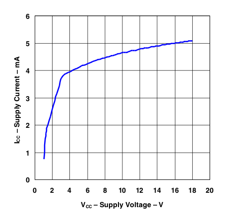 Figure 1. Supply Current vs Supply Voltage
 (TA = 25°C)
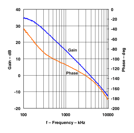 Figure 3. Gain and Phase vs Frequency
(VCC = ±15 V, RL = 2 kΩ, CL = 22 pF)
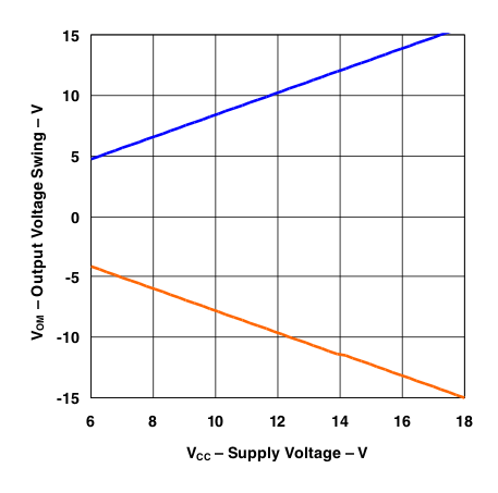 Figure 5. Output Voltage Swing vs Supply Voltage
 (RL = 2 kΩ, TA = 25°C)
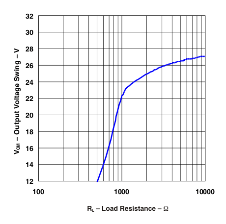 Figure 7. Output Voltage Swing vs Load Resistance
 (VCC = ±15 V, TA = 25°C)
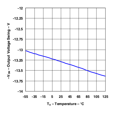 Figure 9. Negative Output Voltage Swing vs Temperature
(VCC = ±15 V, RL = 10 kΩ)
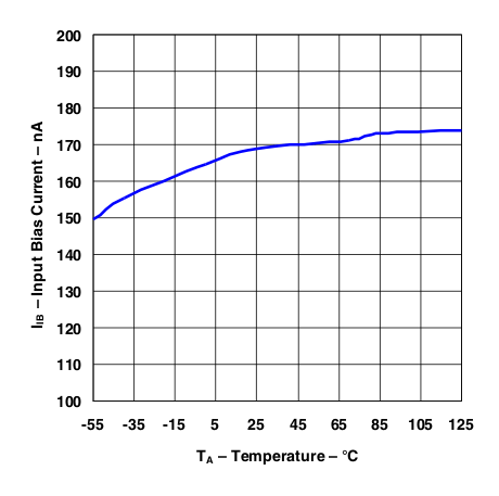 Figure 11. Input Bias Current vs Temperature
(VCC = ±15 V)
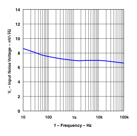 Figure 13. Input Noise Voltage vs Frequency
 (VCC = ±15 V, TA = 25°C)
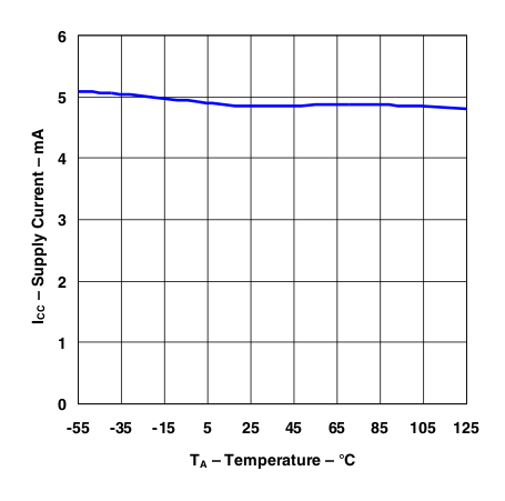 Figure 2. Supply Current vs Temperature
(VCC = ±15 V)
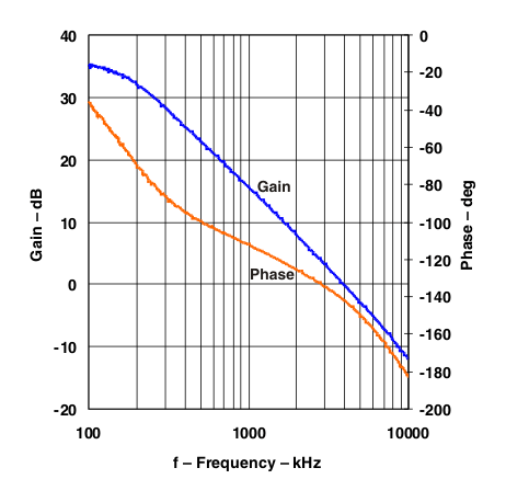 Figure 4. Gain and Phase vs Frequency
(VCC = ±15 V, RL = 10 kΩ, CL = 22 pF)
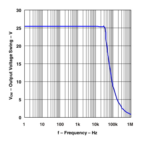 Figure 6. Output Voltage Swing vs Frequency
 (VCC = ±15 V, RL = 2 kΩ, TA = 25°C)
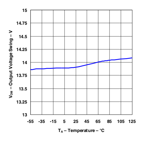 Figure 8. Output Voltage Swing vs Temperature
 (VCC = ±15 V, RL = 10 kΩ)
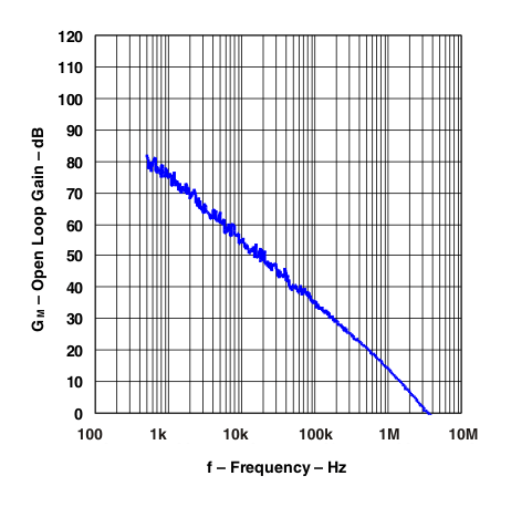 Figure 10. Open Loop Gain vs Frequency
 (VCC = ±15 V, RL = 2 kΩ, CL = 22 pF, TA = 25°C)
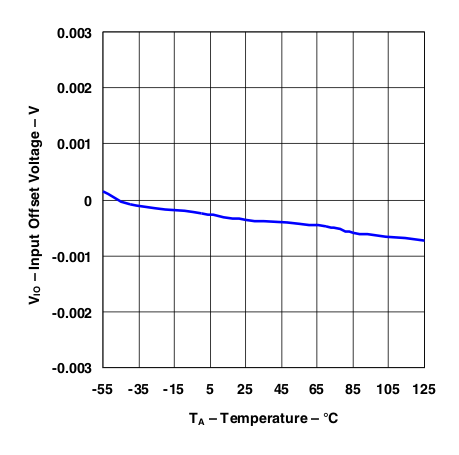 Figure 12. Input Offset Voltage vs Temperature
 (VCC = ±15 V)