SLAS916C November 2012 – November 2014 RF430CL330H
PRODUCTION DATA.
- 1Device Overview
- 2Revision History
- 3Terminal Configuration and Functions
-
4Specifications
- 4.1 Absolute Maximum Ratings
- 4.2 Handling Ratings
- 4.3 Recommended Operating Conditions
- 4.4 Recommended Operating Conditions, Resonant Circuit
- 4.5 Supply Currents
- 4.6 Digital Inputs
- 4.7 Digital Outputs
- 4.8 Thermal Characteristics
- 4.9 Serial Communication Protocol Timings
- 4.10 I2C Interface
- 4.11 SPI Interface
- 4.12 RF143B, Recommended Operating Conditions
- 4.13 RF143B, ISO14443B ASK Demodulator
- 4.14 RF143B, ISO14443B-Compliant Load Modulator
- 4.15 RF143B, Power Supply
- 5Detailed Description
- 6Device and Documentation Support
- 7Mechanical Packaging and Orderable Information
Package Options
Mechanical Data (Package|Pins)
Thermal pad, mechanical data (Package|Pins)
Orderable Information
3 Terminal Configuration and Functions
Figure 3-1 shows the pin assignments for the PW package.
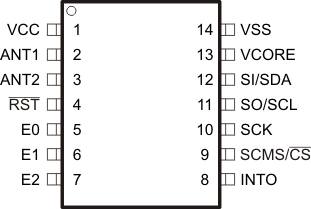 Figure 3-1 14-Pin PW Package (Top View)
Figure 3-2 shows the pin assignments for the RGT package.
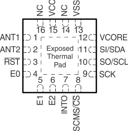
Table 3-1 Terminal Functions
| TERMINAL | I/O | DESCRIPTION | ||
|---|---|---|---|---|
| NAME | NO. | |||
| PW | RGT | |||
| VCC | 1 | 15 | PWR |
3.3-V power supply |
| ANT1 | 2 | 1 | RF |
Antenna input 1 |
| ANT2 | 3 | 2 | RF |
Antenna input 2 |
| RST | 4 | 3 | I |
Reset input (active low) |
| E0 (TMS) | 5 | 4 | I |
I2C address select 0 SPI mode select 0 (JTAG test mode select) |
| E1 (TDO) | 6 | 5 | I (O) |
I2C address select 1 SPI mode select 1 (JTAG test data output) |
| E2 (TDI) | 7 | 6 | I |
I2C address select 2 (JTAG test data in) |
| INTO (TCK) | 8 | 7 | O |
Interrupt output (JTAG test clock) |
|
SCMS/ CS |
9 | 8 | I |
Serial Communication Mode Select (during device initialization) Chip select (in SPI mode) |
| SCK | 10 | 9 | I |
SPI clock input (SPI mode) |
| SO/SCL | 11 | 10 | I/O |
SPI slave out (SPI mode) I2C clock (I2C mode) |
| SI/SDA | 12 | 11 | I/O |
SPI slave in (SPI mode) I2C data (I2C mode) |
| VCORE | 13 | 12 | PWR |
Regulated core supply voltage |
| VSS | 14 | 13 | PWR |
Ground supply |
| NC | - | 14, 16 | Leave open, No connection | |
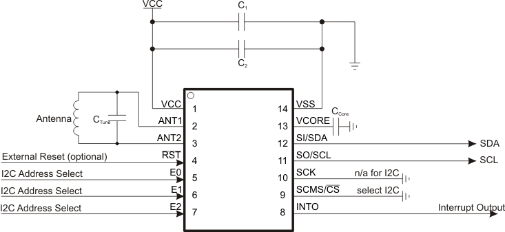
For recommended capacitance values, see Recommended Operating Conditions.
Figure 3-3 Example Application Diagram (I2C Operation) (PW Package Shown)
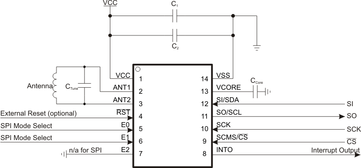
For recommended capacitance values, see Recommended Operating Conditions.
Figure 3-4 Example Application Diagram (SPI Operation) (PW Package Shown)