SLAS740A January 2013 – October 2015 RF430F5978
PRODUCTION DATA.
- 1Device Overview
- 2Revision History
- 3Device Characteristics
- 4Terminal Configuration and Functions
-
5Specifications
- 5.1 Absolute Maximum Ratings
- 5.2 ESD Ratings
- 5.3 Recommended Operating Conditions
- 5.4 Active Mode Supply Current Into VCC Excluding External Current
- 5.5 Typical Characteristics - Active Mode Supply Currents
- 5.6 Low-Power Mode Supply Currents (Into VCC) Excluding External Current
- 5.7 Typical Characteristics - Low-Power Mode Supply Currents
- 5.8 Thermal Resistance Characteristics
- 5.9 Digital Inputs
- 5.10 Digital Outputs
- 5.11 Typical Characteristics - Outputs, Reduced Drive Strength (PxDS.y = 0)
- 5.12 Typical Characteristics - Outputs, Full Drive Strength (PxDS.y = 1)
- 5.13 Crystal Oscillator, XT1, Low-Frequency Mode
- 5.14 Internal Very-Low-Power Low-Frequency Oscillator (VLO)
- 5.15 Internal Reference, Low-Frequency Oscillator (REFO)
- 5.16 DCO Frequency
- 5.17 PMM, Brown-Out Reset (BOR)
- 5.18 PMM, Core Voltage
- 5.19 PMM, SVS High Side
- 5.20 PMM, SVM High Side
- 5.21 PMM, SVS Low Side
- 5.22 PMM, SVM Low Side
- 5.23 Wake-up Times From Low-Power Modes and Reset
- 5.24 Timer_A
- 5.25 USCI (UART Mode) Clock Frequency
- 5.26 USCI (UART Mode)
- 5.27 USCI (SPI Master Mode) Clock Frequency
- 5.28 USCI (SPI Master Mode)
- 5.29 USCI (SPI Slave Mode)
- 5.30 USCI (I2C Mode)
- 5.31 12-Bit ADC, Power Supply and Input Range Conditions
- 5.32 12-Bit ADC, Timing Parameters
- 5.33 12-Bit ADC, Linearity Parameters
- 5.34 12-Bit ADC, Temperature Sensor and Built-In VMID
- 5.35 REF, External Reference
- 5.36 REF, Built-In Reference
- 5.37 Comparator B
- 5.38 Flash Memory
- 5.39 JTAG and Spy-Bi-Wire Interface
- 5.40
RF1A CC1101 Radio Parameters
- 5.40.1 RF Crystal Oscillator, XT2
- 5.40.2 Current Consumption, Reduced-Power Modes
- 5.40.3 Current Consumption, Receive Mode
- 5.40.4 Current Consumption, Transmit Mode
- 5.40.5 Typical TX Current Consumption, 315 MHz
- 5.40.6 Typical TX Current Consumption, 433 MHz
- 5.40.7 Typical TX Current Consumption, 868 MHz
- 5.40.8 Typical TX Current Consumption, 915 MHz
- 5.40.9 RF Receive, Overall
- 5.40.10 RF Receive, 315 MHz
- 5.40.11 RF Receive, 433 MHz
- 5.40.12 RF Receive, 868 or 915 MHz
- 5.40.13 Typical Sensitivity, 315 MHz, Sensitivity-Optimized Setting
- 5.40.14 Typical Sensitivity, 433 MHz, Sensitivity-Optimized Setting
- 5.40.15 Typical Sensitivity, 868 MHz, Sensitivity-Optimized Setting
- 5.40.16 Typical Sensitivity, 915 MHz, Sensitivity-Optimized Setting
- 5.40.17 RF Transmit
- 5.40.18 Optimum PATABLE Settings for Various Output Power Levels and Frequency Bands
- 5.40.19 Typical Output Power, 315 MHz
- 5.40.20 Typical Output Power, 433 MHz
- 5.40.21 Typical Output Power, 868 MHz
- 5.40.22 Typical Output Power, 915 MHz
- 5.40.23 Frequency Synthesizer Characteristics
- 5.40.24 Typical RSSI_offset Values
- 5.41
3D LF Front-End Parameters
- 5.41.1 Recommended Operating Conditions
- 5.41.2 Resonant Circuits - LF Front End
- 5.41.3 External Antenna Coil - LF Front End
- 5.41.4 Resonant Circuit Capacitor - LF Front End
- 5.41.5 Charge Capacitor - LF Front End
- 5.41.6 LF Wake Receiver Electrical Characteristics
- 5.41.7 RSSI - LF Wake Receiver Electrical Characteristics
-
6Detailed Description
- 6.1 3D LF Wake Receiver and 3D Transponder Interface
- 6.2 Sub-1-GHz Radio
- 6.3 CPU
- 6.4 Operating Modes
- 6.5 Interrupt Vector Addresses
- 6.6 Memory Organization
- 6.7 Bootloader (BSL)
- 6.8 JTAG Operation
- 6.9 Flash Memory
- 6.10 RAM
- 6.11
Peripherals
- 6.11.1 Oscillator and System Clock
- 6.11.2 Power-Management Module (PMM)
- 6.11.3 Digital I/O
- 6.11.4 Port Mapping Controller
- 6.11.5 System (SYS) Module
- 6.11.6 DMA Controller
- 6.11.7 Watchdog Timer (WDT_A)
- 6.11.8 CRC16
- 6.11.9 Hardware Multiplier
- 6.11.10 AES128 Accelerator
- 6.11.11 Universal Serial Communication Interface (USCI)
- 6.11.12 TA0
- 6.11.13 TA1
- 6.11.14 Real-Time Clock (RTC_A)
- 6.11.15 REF Voltage Reference
- 6.11.16 Comparator_B
- 6.11.17 ADC12_A
- 6.11.18 Embedded Emulation Module (EEM) (S Version)
- 6.11.19 Peripheral File Map
- 6.12
Input/Output Schematics
- 6.12.1 Port P1, P1.0 to P1.4, Input/Output With Schmitt Trigger
- 6.12.2 Port P1, P1.5 to P1.7, Input/Output With Schmitt Trigger
- 6.12.3 Port P2, P2.0 to P2.2, Input/Output With Schmitt Trigger
- 6.12.4 Port P2, P2.4 and P2.5, Input/Output With Schmitt Trigger
- 6.12.5 Port P3, P3.1 to P3.3, P3.5, and P3.7, Input/Output With Schmitt Trigger
- 6.12.6 Port P4, P4.0 to P4.2, Input/Output With Schmitt Trigger
- 6.12.7 Port P5, P5.0, Input/Output With Schmitt Trigger
- 6.12.8 Port P5, P5.1, Input/Output With Schmitt Trigger
- 6.12.9 Port J, J.0 JTAG Pin TDO, Input/Output With Schmitt Trigger or Output
- 6.12.10 Port J, J.1 to J.3 JTAG Pins TMS, TCK, TDI/TCLK, Input/Output With Schmitt Trigger or Output
- 6.13 Device Descriptor Structures
- 7Applications, Implementation, and Layout
- 8Device and Documentation Support
- 9Mechanical, Packaging, and Orderable Information
Package Options
Mechanical Data (Package|Pins)
- RGC|64
Thermal pad, mechanical data (Package|Pins)
- RGC|64
Orderable Information
5 Specifications
5.1 Absolute Maximum Ratings(1)
over operating free-air temperature range (unless otherwise noted)| MIN | MAX | UNIT | ||
|---|---|---|---|---|
| Voltage applied at DVCC/VBAT and AVCC pins to VSS | –0.3 | 3.6 | V | |
| Voltage applied to any pin (excluding VCORE, RF_P, RF_N, and R_BIAS)(2) | –0.3 | VCC + 0.3 4.1 V Max |
V | |
| Voltage applied to VCORE, RF_P, RF_N, and R_BIAS(2) | –0.3 | 2 | V | |
| Input RF level at pins RF_P and RF_N | 10 | dBm | ||
| Diode current at any device terminal | ±2 | mA | ||
| Storage temperature(3), Tstg | –55 | 125 | °C | |
| Maximum junction temperature, TJ | 95 | °C | ||
(1) Stresses beyond those listed under Absolute Maximum Ratings may cause permanent damage to the device. These are stress ratings only, and functional operation of the device at these or any other conditions beyond those indicated under Recommended Operating Conditions is not implied. Exposure to absolute-maximum-rated conditions for extended periods may affect device reliability.
(2) All voltages referenced to VSS.
(3) Higher temperature may be applied during board soldering according to the current JEDEC J-STD-020 specification with peak reflow temperatures not higher than classified on the device label on the shipping boxes or reels.
5.2 ESD Ratings
| VALUE | UNIT | |||
|---|---|---|---|---|
| V(ESD) | Electrostatic discharge | Human-body model (HBM), per ANSI/ESDA/JEDEC JS-001(1) | ±1000 | V |
| Charged-device model (CDM), per JEDEC specification JESD22-C101(2) | ±250 | |||
(1) JEDEC document JEP155 states that 500-V HBM allows safe manufacturing with a standard ESD control process. Pins listed as ±1000 V may actually have higher performance.
(2) JEDEC document JEP157 states that 250-V CDM allows safe manufacturing with a standard ESD control process. Pins listed as ±250 V may actually have higher performance.
5.3 Recommended Operating Conditions
Typical values are specified at VCC = 3.3 V and TA = 25°C (unless otherwise noted)| MIN | NOM | MAX | UNIT | |||
|---|---|---|---|---|---|---|
| VCC | Supply voltage range applied at all DVCC and AVCC pins(1) during program execution and flash programming with PMM default settings. Radio is not operational with PMMCOREVx = 0, 1.(3)(4) | PMMCOREVx = 0 (default after POR) |
1.8 | 3.6 | V | |
| PMMCOREVx = 1 | 2.0 | 3.6 | ||||
| VCC | Supply voltage range applied at all DVCC and AVCC pins(1) during program execution, flash programming, and radio operation with PMM default settings.(3)(4) | PMMCOREVx = 2 | 2.2 | 3.6 | V | |
| PMMCOREVx = 3 | 2.4 | 3.6 | ||||
| VCC | Supply voltage range applied at all DVCC and AVCC pins(1) during program execution, flash programming, and radio operation with PMMCOREVx = 2, high-side SVS level lowered (SVSHRVLx = SVSHRRRLx = 1) or high-side SVS disabled (SVSHE = 0).(5) (3)(4) | PMMCOREVx = 2, SVSHRVLx = SVSHRRRLx = 1 or SVSHE = 0 |
2.0 | 3.6 | V | |
| VSS | Supply voltage applied at the exposed die attach VSS and AVSS pin | 0 | V | |||
| TA | Operating free-air temperature | –40 | 85 | °C | ||
| TJ | Operating junction temperature | –40 | 85 | °C | ||
| CVCORE | Recommended capacitor at VCORE(2) | 470 | nF | |||
| CDVCC/ CVCORE | Capacitor ratio of capacitor at DVCC to capacitor at VCORE | 10 | ||||
| fSYSTEM | Processor (MCLK) frequency(6) (see Figure 5-1) | PMMCOREVx = 0 (default condition) |
0 | 8 | MHz | |
| PMMCOREVx = 1 | 0 | 12 | ||||
| PMMCOREVx = 2 | 0 | 16 | ||||
| PMMCOREVx = 3 | 0 | 20 | ||||
| PINT | Internal power dissipation | VCC × I(DVCC) | W | |||
| PIO | I/O power dissipation of I/O pins powered by DVCC | (VCC – VIOH) × IIOH + VIOL × IIOL |
W | |||
| PMAX | Maximum allowed power dissipation, PMAX > PIO + PINT | (TJ – TA) / RθJA | W | |||
(1) TI recommends powering AVCC and DVCC from the same source. A maximum difference of 0.3 V between AVCC and DVCC can be tolerated during power up and operation.
(2) A capacitor tolerance of ±20% or better is required.
(3) Modules may have a different supply voltage range specification. See the specification of the respective module in this data sheet.
(4) The minimum supply voltage is defined by the supervisor SVS levels when it is enabled. See the Section 5.19 threshold parameters for the exact values and further details.
(5) Lowering the high-side SVS level or disabling the high-side SVS might cause the LDO to operate out of regulation, but the core voltage stays within its limits and is still supervised by the low-side SVS to ensure reliable operation.
(6) Modules may have a different maximum input clock specification. See the specification of the respective module in this data sheet.
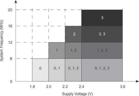
A.
Figure 5-1 Maximum System Frequency
NOTE:
The numbers (0, 1, 2, and 3) in the fields are the supported PMMCOREVx settings.5.4 Active Mode Supply Current Into VCC Excluding External Current
over recommended operating free-air temperature (unless otherwise noted)(1) (2) (3)| PARAMETER | EXECUTION MEMORY | VCC | PMMCOREVx | FREQUENCY (fDCO = fMCLK = fSMCLK) | UNIT | |||||||||
|---|---|---|---|---|---|---|---|---|---|---|---|---|---|---|
| 1 MHz | 8 MHz | 12 MHz | 16 MHz | 20 MHz | ||||||||||
| TYP | MAX | TYP | MAX | TYP | MAX | TYP | MAX | TYP | MAX | |||||
| IAM, Flash(4) | Flash | 3 V | 0 | 0.23 | 0.26 | 1.35 | 1.60 | mA | ||||||
| 1 | 0.25 | 0.28 | 1.55 | 2.30 | 2.65 | |||||||||
| 2 | 0.27 | 0.30 | 1.75 | 2.60 | 3.45 | 3.90 | ||||||||
| 3 | 0.28 | 0.32 | 1.85 | 2.75 | 3.65 | 4.55 | 5.10 | |||||||
| IAM, RAM(5) | RAM | 3 V | 0 | 0.18 | 0.20 | 0.95 | 1.10 | mA | ||||||
| 1 | 0.20 | 0.22 | 1.10 | 1.60 | 1.85 | |||||||||
| 2 | 0.21 | 0.24 | 1.20 | 1.80 | 2.40 | 2.70 | ||||||||
| 3 | 0.22 | 0.25 | 1.30 | 1.90 | 2.50 | 3.10 | 3.60 | |||||||
(1) All inputs are tied to 0 V or to VCC. Outputs do not source or sink any current.
(2) The currents are characterized with a Micro Crystal MS1V-T1K crystal with a load capacitance of 12.5 pF. The internal and external load capacitance are chosen to closely match the required 12.5 pF.
(3) Characterized with program executing typical data processing.
fACLK = 32786 Hz, fDCO = fMCLK = fSMCLK at specified frequency.
XTS = CPUOFF = SCG0 = SCG1 = OSCOFF = SMCLKOFF = 0.
fACLK = 32786 Hz, fDCO = fMCLK = fSMCLK at specified frequency.
XTS = CPUOFF = SCG0 = SCG1 = OSCOFF = SMCLKOFF = 0.
(4) Active mode supply current when program executes in flash at a nominal supply voltage of 3 V.
(5) Active mode supply current when program executes in RAM at a nominal supply voltage of 3 V.
5.5 Typical Characteristics – Active Mode Supply Currents
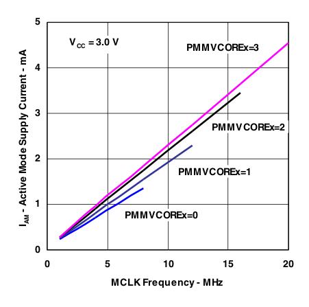 Figure 5-2 Active Mode Supply Current vs MCLK Frequency
5.6 Low-Power Mode Supply Currents (Into VCC) Excluding External Current
over recommended ranges of supply voltage and operating free-air temperature (unless otherwise noted)(1) (2)| PARAMETER | VCC | PMMCOREVx | TEMPERATURE (TA) | UNIT | ||||||||
|---|---|---|---|---|---|---|---|---|---|---|---|---|
| –40°C | 25°C | 60°C | 85°C | |||||||||
| TYP | MAX | TYP | MAX | TYP | MAX | TYP | MAX | |||||
| ILPM0,1MHz | Low-power mode 0(3) (8) | 2.2 V | 0 | 80 | 100 | 80 | 100 | 80 | 100 | 80 | 100 | µA |
| 3 V | 3 | 90 | 110 | 90 | 110 | 90 | 110 | 90 | 110 | |||
| ILPM2 | Low-power mode 2(4) (8) | 2.2 V | 0 | 6.5 | 11 | 6.5 | 11 | 6.5 | 11 | 6.5 | 11 | µA |
| 3 V | 3 | 7.5 | 12 | 7.5 | 12 | 7.5 | 12 | 7.5 | 12 | |||
| ILPM3,XT1LF | Low-power mode 3, crystal mode(5) (8) | 3 V | 0 | 1.8 | 2.0 | 2.6 | 3.0 | 4.0 | 4.4 | 5.9 | µA | |
| 1 | 1.9 | 2.1 | 3.2 | 4.8 | ||||||||
| 2 | 2.0 | 2.2 | 3.4 | 5.1 | ||||||||
| 3 | 2.0 | 2.2 | 2.9 | 3.5 | 4.8 | 5.3 | 7.4 | |||||
| ILPM3,VLO | Low-power mode 3, VLO mode(6) (8) | 3 V | 0 | 0.9 | 1.1 | 2.3 | 2.1 | 3.7 | 3.5 | 5.6 | µA | |
| 1 | 1.0 | 1.2 | 2.3 | 3.9 | ||||||||
| 2 | 1.1 | 1.3 | 2.5 | 4.2 | ||||||||
| 3 | 1.1 | 1.3 | 2.6 | 2.6 | 4.5 | 4.4 | 7.1 | |||||
| ILPM4 | Low-power mode 4(7) (8) | 3 V | 0 | 0.8 | 1.0 | 2.2 | 2.0 | 3.6 | 3.4 | 5.5 | µA | |
| 1 | 0.9 | 1.1 | 2.2 | 3.8 | ||||||||
| 2 | 1.0 | 1.2 | 2.4 | 4.1 | ||||||||
| 3 | 1.0 | 1.2 | 2.5 | 2.5 | 4.4 | 4.3 | 7.0 | |||||
(1) All inputs are tied to 0 V or to VCC. Outputs do not source or sink any current.
(2) The currents are characterized with a Micro Crystal MS1V-T1K crystal with a load capacitance of 12.5 pF. The internal and external load capacitance are chosen to closely match the required 12.5 pF.
(3) Current for watchdog timer clocked by SMCLK included. ACLK = low frequency crystal operation (XTS = 0, XT1DRIVEx = 0).
CPUOFF = 1, SCG0 = 0, SCG1 = 0, OSCOFF = 0 (LPM0), fACLK = 32768 Hz, fMCLK = 0 MHz, fSMCLK = fDCO = 1 MHz
CPUOFF = 1, SCG0 = 0, SCG1 = 0, OSCOFF = 0 (LPM0), fACLK = 32768 Hz, fMCLK = 0 MHz, fSMCLK = fDCO = 1 MHz
(4) Current for watchdog timer and RTC clocked by ACLK included. ACLK = low frequency crystal operation (XTS = 0, XT1DRIVEx = 0).
CPUOFF = 1, SCG0 = 0, SCG1 = 1, OSCOFF = 0 (LPM2), fACLK = 32768 Hz, fMCLK = 0 MHz, fSMCLK = fDCO = 0 MHz, DCO setting = 1 MHz operation, DCO bias generator enabled.
CPUOFF = 1, SCG0 = 0, SCG1 = 1, OSCOFF = 0 (LPM2), fACLK = 32768 Hz, fMCLK = 0 MHz, fSMCLK = fDCO = 0 MHz, DCO setting = 1 MHz operation, DCO bias generator enabled.
(5) Current for watchdog timer and RTC clocked by ACLK included. ACLK = low frequency crystal operation (XTS = 0, XT1DRIVEx = 0).
CPUOFF = 1, SCG0 = 1, SCG1 = 1, OSCOFF = 0 (LPM3), fACLK = 32768 Hz, fMCLK = fSMCLK = fDCO = 0 MHz
CPUOFF = 1, SCG0 = 1, SCG1 = 1, OSCOFF = 0 (LPM3), fACLK = 32768 Hz, fMCLK = fSMCLK = fDCO = 0 MHz
(6) Current for watchdog timer and RTC clocked by ACLK included. ACLK = VLO.
CPUOFF = 1, SCG0 = 1, SCG1 = 1, OSCOFF = 0 (LPM3), fACLK = fVLO, fMCLK = fSMCLK = fDCO = 0 MHz
CPUOFF = 1, SCG0 = 1, SCG1 = 1, OSCOFF = 0 (LPM3), fACLK = fVLO, fMCLK = fSMCLK = fDCO = 0 MHz
(7) CPUOFF = 1, SCG0 = 1, SCG1 = 1, OSCOFF = 1 (LPM4), fDCO = fACLK = fMCLK = fSMCLK = 0 MHz
(8) Current for brownout, high side supervisor (SVSH) normal mode included. Low-side supervisor (SVSL) and low-side monitor (SVML) disabled. High-side monitor (SVMH) disabled. RAM retention enabled.
5.7 Typical Characteristics – Low-Power Mode Supply Currents
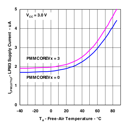 Figure 5-3 LPM3 Supply Current vs Temperature
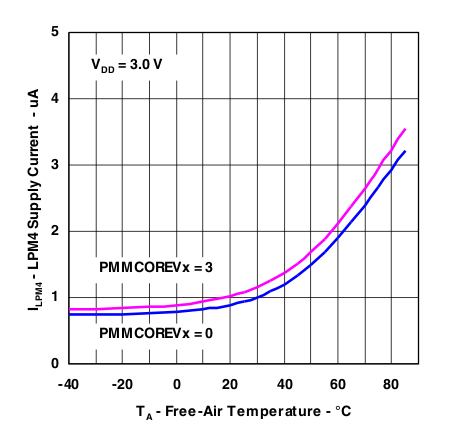 Figure 5-4 LPM4 Supply Current vs Temperature
5.8 Thermal Resistance Characteristics
over operating free-air temperature range (unless otherwise noted)| VALUE | UNIT | |||
|---|---|---|---|---|
| RθJA | Junction-to-ambient thermal resistance, still air(1) | VQFN-64 (RGC) | 24.6 | °C/W |
| RθJC(TOP) | Junction-to-case (top) thermal resistance(2) | 8.8 | °C/W | |
| RθJC(BOT) | Junction-to-case (bottom) thermal resistance(4) | 0.9 | °C/W | |
| RθJB | Junction-to-board thermal resistance(3) | 3.8 | °C/W | |
| ΨJB | Junction-to-board thermal characterization parameter | 3.8 | °C/W | |
| ΨJT | Junction-to-top thermal characterization parameter | 0.1 | °C/W | |
(1) The junction-to-ambient thermal resistance under natural convection is obtained in a simulation on a JEDEC-standard, High-K board, as specified in JESD51-7, in an environment described in JESD51-2a.
(2) The junction-to-case (top) thermal resistance is obtained by simulating a cold plate test on the package top. No specific JEDEC standard test exists, but a close description can be found in the ANSI SEMI standard G30-88.
(3) The junction-to-board thermal resistance is obtained by simulating in an environment with a ring cold plate fixture to control the PCB temperature, as described in JESD51-8.
(4) The junction-to-case (bottom) thermal resistance is obtained by simulating a cold plate test on the exposed (power) pad. No specific JEDEC standard test exists, but a close description can be found in the ANSI SEMI standard G30-88.
5.9 Digital Inputs
over recommended ranges of supply voltage and operating free-air temperature (unless otherwise noted)| PARAMETER | TEST CONDITIONS | VCC | MIN | TYP | MAX | UNIT | |
|---|---|---|---|---|---|---|---|
| VIT+ | Positive-going input threshold voltage | 1.8 V | 0.80 | 1.40 | V | ||
| 3 V | 1.50 | 2.10 | |||||
| VIT– | Negative-going input threshold voltage | 1.8 V | 0.45 | 1.00 | V | ||
| 3 V | 0.75 | 1.65 | |||||
| Vhys | Input voltage hysteresis (VIT+ – VIT–) | 1.8 V | 0.3 | 0.8 | V | ||
| 3 V | 0.4 | 1.0 | |||||
| RPull | Pullup or pulldown resistor | For pullup: VIN = VSS
For pulldown: VIN = VCC |
20 | 35 | 50 | kΩ | |
| CI | Input capacitance | VIN = VSS or VCC | 5 | pF | |||
| Ilkg(Px.y) | High-impedance leakage current | (1) (2) | 1.8 V, 3 V | ±50 | nA | ||
| t(int) | External interrupt timing (external trigger pulse duration to set interrupt flag)(3) | Ports with interrupt capability (see block diagram and terminal function descriptions). | 1.8 V, 3 V | 20 | ns | ||
(1) The leakage current is measured with VSS or VCC applied to the corresponding pin(s), unless otherwise noted.
(2) The leakage of the digital port pins is measured individually. The port pin is selected for input and the pullup or pulldown resistor is disabled.
(3) An external signal sets the interrupt flag every time the minimum interrupt pulse duration t(int) is met. It may be set by trigger signals shorter than t(int).
5.10 Digital Outputs
over recommended ranges of supply voltage and operating free-air temperature (unless otherwise noted)| PARAMETER | TEST CONDITIONS | VCC | MIN | MAX | UNIT | |
|---|---|---|---|---|---|---|
| VOH | High-level output voltage, reduced drive strength(3) | I(OHmax) = –1 mA, PxDS.y = 0(1) | 1.8 V | VCC – 0.25 | VCC | V |
| I(OHmax) = –3 mA, PxDS.y = 0(2) | VCC – 0.60 | VCC | ||||
| I(OHmax) = –2 mA, PxDS.y = 0(1) | 3 V | VCC – 0.25 | VCC | |||
| I(OHmax) = –6 mA, PxDS.y = 0(2) | VCC – 0.60 | VCC | ||||
| VOL | Low-level output voltage, reduced drive strength(3) | I(OLmax) = 1 mA, PxDS.y = 0(1) | 1.8 V | VSS | VSS + 0.25 | V |
| I(OLmax) = 3 mA, PxDS.y = 0(2) | VSS | VSS + 0.60 | ||||
| I(OLmax) = 2 mA, PxDS.y = 0(1) | 3 V | VSS | VSS + 0.25 | |||
| I(OLmax) = 6 mA, PxDS.y = 0(2) | VSS | VSS + 0.60 | ||||
| VOH | High-level output voltage, full drive strength |
I(OHmax) = –3 mA, PxDS.y = 1(1) | 1.8 V | VCC – 0.25 | VCC | V |
| I(OHmax) = –10 mA, PxDS.y = 1(2) | VCC – 0.60 | VCC | ||||
| I(OHmax) = –5 mA, PxDS.y = 1(1) | 3 V | VCC – 0.25 | VCC | |||
| I(OHmax) = –15 mA, PxDS.y = 1(2) | VCC – 0.60 | VCC | ||||
| VOL | Low-level output voltage, full drive strength |
I(OLmax) = 3 mA, PxDS.y = 1(1) | 1.8 V | VSS | VSS + 0.25 | V |
| I(OLmax) = 10 mA, PxDS.y = 1(2) | VSS | VSS + 0.60 | ||||
| I(OLmax) = 5 mA, PxDS.y = 1(1) | 3 V | VSS | VSS + 0.25 | |||
| I(OLmax) = 15 mA, PxDS.y = 1(2) | VSS | VSS + 0.60 | ||||
| fPx.y | Port output frequency (with load) | CL = 20 pF, RL (4) (5) | VCC = 1.8 V, PMMCOREVx = 0 |
16 | MHz | |
| VCC = 3 V, PMMCOREVx = 2 |
25 | |||||
| fPort_CLK | Clock output frequency | CL = 20 pF(5) | VCC = 1.8 V, PMMCOREVx = 0 |
16 | MHz | |
| VCC = 3 V, PMMCOREVx = 2 |
25 | |||||
(1) The maximum total current, I(OHmax) and I(OLmax), for all outputs combined should not exceed ±48 mA to hold the maximum voltage drop specified.
(2) The maximum total current, I(OHmax) and I(OLmax), for all outputs combined should not exceed ±100 mA to hold the maximum voltage drop specified.
(3) Selecting reduced drive strength may reduce EMI.
(4) A resistive divider with 2 × R1 between VCC and VSS is used as load. The output is connected to the center tap of the divider. For full drive strength, R1 = 550 Ω. For reduced drive strength, R1 = 1.6 kΩ. CL = 20 pF is connected to the output to VSS.
(5) The output voltage reaches at least 10% and 90% VCC at the specified toggle frequency.
5.11 Typical Characteristics – Outputs, Reduced Drive Strength (PxDS.y = 0)
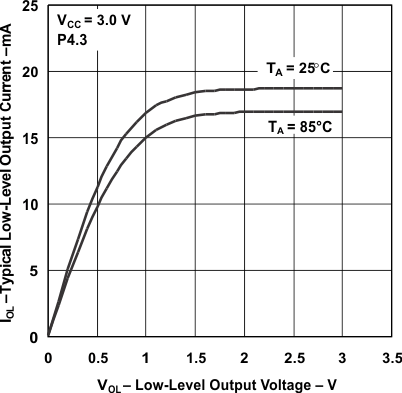 Figure 5-5 Typical Low-Level Output Current vs Low-Level Output Voltage
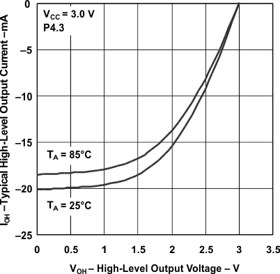 Figure 5-7 Typical High-Level Output Current vs High-Level Output Voltage
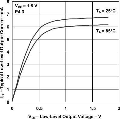 Figure 5-6 Typical Low-Level Output Current vs Low-Level Output Voltage
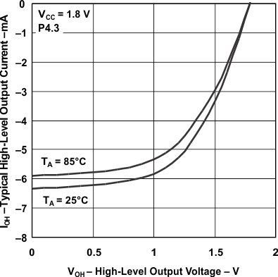 Figure 5-8 Typical High-Level Output Current vs High-Level Output Voltage
5.12 Typical Characteristics – Outputs, Full Drive Strength (PxDS.y = 1)
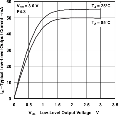 Figure 5-9 Typical Low-Level Output Current vs Low-Level Output Voltage
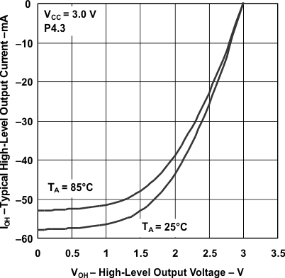 Figure 5-11 Typical High-Level Output Current vs High-Level Output Voltage
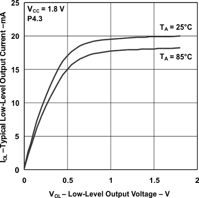 Figure 5-10 Typical Low-Level Output Current vs Low-Level Output Voltage
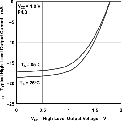 Figure 5-12 Typical High-Level Output Current vs High-Level Output Voltage
5.13 Crystal Oscillator, XT1, Low-Frequency Mode(5)
over recommended ranges of supply voltage and operating free-air temperature (unless otherwise noted)| PARAMETER | TEST CONDITIONS | VCC | MIN | TYP | MAX | UNIT | |
|---|---|---|---|---|---|---|---|
| ΔIDVCC.LF | Differential XT1 oscillator crystal current consumption from lowest drive setting, LF mode | fOSC = 32768 Hz, XTS = 0, XT1BYPASS = 0, XT1DRIVEx = 1, TA = 25°C |
3 V | 0.075 | µA | ||
| fOSC = 32768 Hz, XTS = 0, XT1BYPASS = 0, XT1DRIVEx = 2, TA = 25°C |
0.170 | ||||||
| fOSC = 32768 Hz, XTS = 0, XT1BYPASS = 0, XT1DRIVEx = 3, TA = 25°C |
0.290 | ||||||
| fXT1,LF0 | XT1 oscillator crystal frequency, LF mode | XTS = 0, XT1BYPASS = 0 | 32768 | Hz | |||
| fXT1,LF,SW | XT1 oscillator logic-level square-wave input frequency, LF mode | XTS = 0, XT1BYPASS = 1(6) (7) | 10 | 32.768 | 50 | kHz | |
| OALF | Oscillation allowance for LF crystals(8) | XTS = 0, XT1BYPASS = 0, XT1DRIVEx = 0, fXT1,LF = 32768 Hz, CL,eff = 6 pF |
210 | kΩ | |||
| XTS = 0, XT1BYPASS = 0, XT1DRIVEx = 1, fXT1,LF = 32768 Hz, CL,eff = 12 pF |
300 | ||||||
| CL,eff | Integrated effective load capacitance, LF mode(1) | XTS = 0, XCAPx = 0(2) | 2 | pF | |||
| XTS = 0, XCAPx = 1 | 5.5 | ||||||
| XTS = 0, XCAPx = 2 | 8.5 | ||||||
| XTS = 0, XCAPx = 3 | 12.0 | ||||||
| Duty cycle, LF mode | XTS = 0, Measured at ACLK, fXT1,LF = 32768 Hz |
30% | 70% | ||||
| fFault,LF | Oscillator fault frequency, LF mode(4) | XTS = 0(3) | 10 | 10000 | Hz | ||
| tSTART,LF | Start-up time, LF mode | fOSC = 32768 Hz, XTS = 0, XT1BYPASS = 0, XT1DRIVEx = 0, TA = 25°C, CL,eff = 6 pF |
3 V | 1000 | ms | ||
| fOSC = 32768 Hz, XTS = 0, XT1BYPASS = 0, XT1DRIVEx = 3, TA = 25°C, CL,eff = 12 pF |
500 | ||||||
(1) Includes parasitic bond and package capacitance (approximately 2 pF per pin).
Because the PCB adds additional capacitance, TI recommends verifying the correct load by measuring the ACLK frequency. For a correct setup, the effective load capacitance should always match the specification of the used crystal.
Because the PCB adds additional capacitance, TI recommends verifying the correct load by measuring the ACLK frequency. For a correct setup, the effective load capacitance should always match the specification of the used crystal.
(2) Requires external capacitors at both terminals. Values are specified by crystal manufacturers.
(3) Measured with logic-level input frequency but also applies to operation with crystals.
(4) Frequencies below the MIN specification set the fault flag. Frequencies above the MAX specification do not set the fault flag. Frequencies in between might set the flag.
(5) To improve EMI on the XT1 oscillator, the following guidelines should be observed.
- Keep the trace between the device and the crystal as short as possible.
- Design a good ground plane around the oscillator pins.
- Prevent crosstalk from other clock or data lines into oscillator pins XIN and XOUT.
- Avoid running PCB traces underneath or adjacent to the XIN and XOUT pins.
- Use assembly materials and processes that avoid any parasitic load on the oscillator XIN and XOUT pins.
- If conformal coating is used, make sure that it does not induce capacitive or resistive leakage between the oscillator pins.
(6) When XT1BYPASS is set, XT1 circuits are automatically powered down. Input signal is a digital square wave with parametrics defined in the Schmitt-trigger Inputs section of this datasheet.
(7) Maximum frequency of operation of the entire device cannot be exceeded.
(8) Oscillation allowance is based on a safety factor of 5 for recommended crystals. The oscillation allowance is a function of the XT1DRIVEx settings and the effective load. In general, comparable oscillator allowance can be achieved based on the following guidelines, but should be evaluated based on the actual crystal selected for the application:
- For XT1DRIVEx = 0, CL,eff ≤ 6 pF
- For XT1DRIVEx = 1, 6 pF ≤ CL,eff ≤ 9 pF
- For XT1DRIVEx = 2, 6 pF ≤ CL,eff ≤ 10 pF
- For XT1DRIVEx = 3, CL,eff ≥ 6 pF
5.14 Internal Very-Low-Power Low-Frequency Oscillator (VLO)
over recommended ranges of supply voltage and operating free-air temperature (unless otherwise noted)| PARAMETER | TEST CONDITIONS | VCC | MIN | TYP | MAX | UNIT | |
|---|---|---|---|---|---|---|---|
| fVLO | VLO frequency | Measured at ACLK | 1.8 V to 3.6 V | 6 | 9.4 | 14 | kHz |
| dfVLO/dT | VLO frequency temperature drift | Measured at ACLK(1) | 1.8 V to 3.6 V | 0.5 | %/°C | ||
| dfVLO/dVCC | VLO frequency supply voltage drift | Measured at ACLK(2) | 1.8 V to 3.6 V | 4 | %/V | ||
| Duty cycle | Measured at ACLK | 1.8 V to 3.6 V | 40% | 50% | 60% | ||
(1) Calculated using the box method: (MAX(–40°C to 85°C) – MIN(–40°C to 85°C)) / MIN(–40°C to 85°C) / (85°C – (–40°C))
(2) Calculated using the box method: (MAX(1.8 V to 3.6 V) – MIN(1.8 V to 3.6 V)) / MIN(1.8 V to 3.6 V) / (3.6 V – 1.8 V)
5.15 Internal Reference, Low-Frequency Oscillator (REFO)
over recommended ranges of supply voltage and operating free-air temperature (unless otherwise noted)| PARAMETER | TEST CONDITIONS | VCC | MIN | TYP | MAX | UNIT | |
|---|---|---|---|---|---|---|---|
| IREFO | REFO oscillator current consumption | TA = 25°C | 1.8 V to 3.6 V | 3 | µA | ||
| fREFO | REFO frequency calibrated | Measured at ACLK | 1.8 V to 3.6 V | 32768 | Hz | ||
| REFO absolute tolerance calibrated | Full temperature range | 1.8 V to 3.6 V | ±3.5% | ||||
| TA = 25°C | 3 V | ±1.5% | |||||
| dfREFO/dT | REFO frequency temperature drift | Measured at ACLK(1) | 1.8 V to 3.6 V | 0.01 | %/°C | ||
| dfREFO/dVCC | REFO frequency supply voltage drift | Measured at ACLK(2) | 1.8 V to 3.6 V | 1.0 | %/V | ||
| Duty cycle | Measured at ACLK | 1.8 V to 3.6 V | 40% | 50% | 60% | ||
| tSTART | REFO start-up time | 40%/60% duty cycle | 1.8 V to 3.6 V | 25 | µs | ||
(1) Calculated using the box method: (MAX(–40°C to 85°C) – MIN(–40°C to 85°C)) / MIN(–40°C to 85°C) / (85°C – (–40°C))
(2) Calculated using the box method: (MAX(1.8 V to 3.6 V) – MIN(1.8 V to 3.6 V)) / MIN(1.8 V to 3.6 V) / (3.6 V – 1.8 V)
5.16 DCO Frequency
over recommended ranges of supply voltage and operating free-air temperature (unless otherwise noted)| PARAMETER | TEST CONDITIONS | MIN | TYP | MAX | UNIT | |
|---|---|---|---|---|---|---|
| fDCO(0,0) | DCO frequency (0, 0)(1) | DCORSELx = 0, DCOx = 0, MODx = 0 | 0.07 | 0.20 | MHz | |
| fDCO(0,31) | DCO frequency (0, 31)(1) | DCORSELx = 0, DCOx = 31, MODx = 0 | 0.70 | 1.70 | MHz | |
| fDCO(1,0) | DCO frequency (1, 0)(1) | DCORSELx = 1, DCOx = 0, MODx = 0 | 0.15 | 0.36 | MHz | |
| fDCO(1,31) | DCO frequency (1, 31)(1) | DCORSELx = 1, DCOx = 31, MODx = 0 | 1.47 | 3.45 | MHz | |
| fDCO(2,0) | DCO frequency (2, 0)(1) | DCORSELx = 2, DCOx = 0, MODx = 0 | 0.32 | 0.75 | MHz | |
| fDCO(2,31) | DCO frequency (2, 31)(1) | DCORSELx = 2, DCOx = 31, MODx = 0 | 3.17 | 7.38 | MHz | |
| fDCO(3,0) | DCO frequency (3, 0)(1) | DCORSELx = 3, DCOx = 0, MODx = 0 | 0.64 | 1.51 | MHz | |
| fDCO(3,31) | DCO frequency (3, 31)(1) | DCORSELx = 3, DCOx = 31, MODx = 0 | 6.07 | 14.0 | MHz | |
| fDCO(4,0) | DCO frequency (4, 0)(1) | DCORSELx = 4, DCOx = 0, MODx = 0 | 1.3 | 3.2 | MHz | |
| fDCO(4,31) | DCO frequency (4, 31)(1) | DCORSELx = 4, DCOx = 31, MODx = 0 | 12.3 | 28.2 | MHz | |
| fDCO(5,0) | DCO frequency (5, 0)(1) | DCORSELx = 5, DCOx = 0, MODx = 0 | 2.5 | 6.0 | MHz | |
| fDCO(5,31) | DCO frequency (5, 31)(1) | DCORSELx = 5, DCOx = 31, MODx = 0 | 23.7 | 54.1 | MHz | |
| fDCO(6,0) | DCO frequency (6, 0)(1) | DCORSELx = 6, DCOx = 0, MODx = 0 | 4.6 | 10.7 | MHz | |
| fDCO(6,31) | DCO frequency (6, 31)(1) | DCORSELx = 6, DCOx = 31, MODx = 0 | 39.0 | 88.0 | MHz | |
| fDCO(7,0) | DCO frequency (7, 0)(1) | DCORSELx = 7, DCOx = 0, MODx = 0 | 8.5 | 19.6 | MHz | |
| fDCO(7,31) | DCO frequency (7, 31)(1) | DCORSELx = 7, DCOx = 31, MODx = 0 | 60 | 135 | MHz | |
| SDCORSEL | Frequency step between range DCORSEL and DCORSEL + 1 | SRSEL = fDCO(DCORSEL+1,DCO)/fDCO(DCORSEL,DCO) | 1.2 | 2.3 | ratio | |
| SDCO | Frequency step between tap DCO and DCO + 1 | SDCO = fDCO(DCORSEL,DCO+1)/fDCO(DCORSEL,DCO) | 1.02 | 1.12 | ratio | |
| Duty cycle | Measured at SMCLK | 40% | 50% | 60% | ||
| dfDCO/dT | DCO frequency temperature drift | fDCO = 1 MHz | 0.1 | %/°C | ||
| dfDCO/dVCC | DCO frequency voltage drift | fDCO = 1 MHz | 1.9 | %/V | ||
(1) When selecting the proper DCO frequency range (DCORSELx), the target DCO frequency, fDCO, should be set to reside within the range of fDCO(n, 0),MAX ≤ fDCO ≤ fDCO(n, 31),MIN, where fDCO(n, 0),MAX represents the maximum frequency specified for the DCO frequency, range n, tap 0 (DCOx = 0) and fDCO(n,31),MIN represents the minimum frequency specified for the DCO frequency, range n, tap 31 (DCOx = 31). This ensures that the target DCO frequency resides within the range selected. It should also be noted that if the actual fDCO frequency for the selected range causes the FLL or the application to select tap 0 or 31, the DCO fault flag is set to report that the selected range is at its minimum or maximum tap setting.
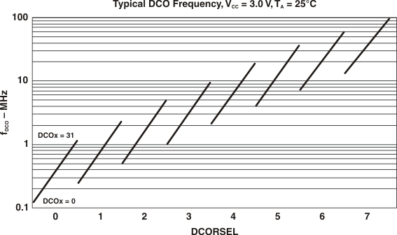 Figure 5-13 Typical DCO frequency
5.17 PMM, Brown-Out Reset (BOR)
over recommended ranges of supply voltage and operating free-air temperature (unless otherwise noted)| PARAMETER | TEST CONDITIONS | MIN | TYP | MAX | UNIT | |
|---|---|---|---|---|---|---|
| V(DVCC_BOR_IT–) | BORH on voltage, DVCC falling level | | dDVCC/dt | < 3 V/s | 1.45 | V | ||
| V(DVCC_BOR_IT+) | BORH off voltage, DVCC rising level | | dDVCC/dt | < 3 V/s | 0.80 | 1.30 | 1.50 | V |
| V(DVCC_BOR_hys) | BORH hysteresis | 60 | 250 | mV | ||
| tRESET | Pulse duration required at RST/NMI pin to accept a reset | 2 | µs | |||
5.18 PMM, Core Voltage
over recommended ranges of supply voltage and operating free-air temperature (unless otherwise noted)| PARAMETER | TEST CONDITIONS | MIN | TYP | MAX | UNIT | |
|---|---|---|---|---|---|---|
| VCORE3(AM) | Core voltage, active mode, PMMCOREV = 3 | 2.4 V ≤ DVCC ≤ 3.6 V | 1.90 | V | ||
| VCORE2(AM) | Core voltage, active mode, PMMCOREV = 2 | 2.2 V ≤ DVCC ≤ 3.6 V | 1.80 | V | ||
| VCORE1(AM) | Core voltage, active mode, PMMCOREV = 1 | 2 V ≤ DVCC ≤ 3.6 V | 1.60 | V | ||
| VCORE0(AM) | Core voltage, active mode, PMMCOREV = 0 | 1.8 V ≤ DVCC ≤ 3.6 V | 1.40 | V | ||
| VCORE3(LPM) | Core voltage, low-current mode, PMMCOREV = 3 | 2.4 V ≤ DVCC ≤ 3.6 V | 1.94 | V | ||
| VCORE2(LPM) | Core voltage, low-current mode, PMMCOREV = 2 | 2.2 V ≤ DVCC ≤ 3.6 V | 1.84 | V | ||
| VCORE1(LPM) | Core voltage, low-current mode, PMMCOREV = 1 | 2 V ≤ DVCC ≤ 3.6 V | 1.64 | V | ||
| VCORE0(LPM) | Core voltage, low-current mode, PMMCOREV = 0 | 1.8 V ≤ DVCC ≤ 3.6 V | 1.44 | V | ||
5.19 PMM, SVS High Side
over recommended ranges of supply voltage and operating free-air temperature (unless otherwise noted)| PARAMETER | TEST CONDITIONS | MIN | TYP | MAX | UNIT | |
|---|---|---|---|---|---|---|
| I(SVSH) | SVS current consumption | SVSHE = 0, DVCC = 3.6 V | 0 | nA | ||
| SVSHE = 1, DVCC = 3.6 V, SVSHFP = 0 | 200 | |||||
| SVSHE = 1, DVCC = 3.6 V, SVSHFP = 1 | 1.5 | µA | ||||
| V(SVSH_IT–) | SVSH on voltage level(1) | SVSHE = 1, SVSHRVL = 0 | 1.53 | 1.60 | 1.67 | V |
| SVSHE = 1, SVSHRVL = 1 | 1.73 | 1.80 | 1.87 | |||
| SVSHE = 1, SVSHRVL = 2 | 1.93 | 2.00 | 2.07 | |||
| SVSHE = 1, SVSHRVL = 3 | 2.03 | 2.10 | 2.17 | |||
| V(SVSH_IT+) | SVSH off voltage level(1) | SVSHE = 1, SVSMHRRL = 0 | 1.60 | 1.70 | 1.80 | V |
| SVSHE = 1, SVSMHRRL = 1 | 1.80 | 1.90 | 2.00 | |||
| SVSHE = 1, SVSMHRRL = 2 | 2.00 | 2.10 | 2.20 | |||
| SVSHE = 1, SVSMHRRL = 3 | 2.10 | 2.20 | 2.30 | |||
| SVSHE = 1, SVSMHRRL = 4 | 2.25 | 2.35 | 2.50 | |||
| SVSHE = 1, SVSMHRRL = 5 | 2.52 | 2.65 | 2.78 | |||
| SVSHE = 1, SVSMHRRL = 6 | 2.85 | 3.00 | 3.15 | |||
| SVSHE = 1, SVSMHRRL = 7 | 2.85 | 3.00 | 3.15 | |||
| tpd(SVSH) | SVSH propagation delay | SVSHE = 1, dVDVCC/dt = 10 mV/µs, SVSHFP = 1 |
2.5 | µs | ||
| SVSHE = 1, dVDVCC/dt = 1 mV/µs, SVSHFP = 0 |
20 | |||||
| t(SVSH) | SVSH on or off delay time | SVSHE = 0 → 1, dVDVCC/dt = 10 mV/µs, SVSHFP = 1 |
12.5 | µs | ||
| SVSHE = 0 → 1, dVDVCC/dt = 1 mV/µs, SVSHFP = 0 |
100 | |||||
| dVDVCC/dt | DVCC rise time | 0 | 1000 | V/s | ||
(1) The SVSH settings available depend on the VCORE (PMMCOREVx) setting. See the Power Management Module and Supply Voltage Supervisor chapter in the RF430F5978 User's Guide (SLAU378) on recommended settings and usage.
5.20 PMM, SVM High Side
over recommended ranges of supply voltage and operating free-air temperature (unless otherwise noted)| PARAMETER | TEST CONDITIONS | MIN | TYP | MAX | UNIT | |
|---|---|---|---|---|---|---|
| I(SVMH) | SVMH current consumption | SVMHE = 0, DVCC = 3.6 V | 0 | nA | ||
| SVMHE = 1, DVCC = 3.6 V, SVMHFP = 0 | 200 | |||||
| SVMHE = 1, DVCC = 3.6 V, SVMHFP = 1 | 1.5 | µA | ||||
| V(SVMH) | SVMH on or off voltage level(1) | SVMHE = 1, SVSMHRRL = 0 | 1.60 | 1.70 | 1.80 | V |
| SVMHE = 1, SVSMHRRL = 1 | 1.80 | 1.90 | 2.00 | |||
| SVMHE = 1, SVSMHRRL = 2 | 2.00 | 2.10 | 2.20 | |||
| SVMHE = 1, SVSMHRRL = 3 | 2.10 | 2.20 | 2.30 | |||
| SVMHE = 1, SVSMHRRL = 4 | 2.25 | 2.35 | 2.50 | |||
| SVMHE = 1, SVSMHRRL = 5 | 2.52 | 2.65 | 2.78 | |||
| SVMHE = 1, SVSMHRRL = 6 | 2.85 | 3.00 | 3.15 | |||
| SVMHE = 1, SVSMHRRL = 7 | 2.85 | 3.00 | 3.15 | |||
| SVMHE = 1, SVMHOVPE = 1 | 3.75 | |||||
| tpd(SVMH) | SVMH propagation delay | SVMHE = 1, dVDVCC/dt = 10 mV/µs, SVMHFP = 1 |
2.5 | µs | ||
| SVMHE = 1, dVDVCC/dt = 1 mV/µs, SVMHFP = 0 |
20 | |||||
| t(SVMH) | SVMH on or off delay time | SVMHE = 0 → 1, dVDVCC/dt = 10 mV/µs, SVMHFP = 1 |
12.5 | µs | ||
| SVMHE = 0 → 1, dVDVCC/dt = 1 mV/µs, SVMHFP = 0 |
100 | |||||
(1) The SVMH settings available depend on the VCORE (PMMCOREVx) setting. See the Power Management Module and Supply Voltage Supervisor chapter in the RF430F5978 User's Guide (SLAU378) on recommended settings and usage.
5.21 PMM, SVS Low Side
over recommended ranges of supply voltage and operating free-air temperature (unless otherwise noted)| PARAMETER | TEST CONDITIONS | MIN | TYP | MAX | UNIT | |
|---|---|---|---|---|---|---|
| I(SVSL) | SVSL current consumption | SVSLE = 0, PMMCOREV = 2 | 0 | nA | ||
| SVSLE = 1, PMMCOREV = 2, SVSLFP = 0 | 200 | |||||
| SVSLE = 1, PMMCOREV = 2, SVSLFP = 1 | 1.5 | µA | ||||
| tpd(SVSL) | SVSL propagation delay | SVSLE = 1, dVCORE/dt = 10 mV/µs, SVSLFP = 1 |
2.5 | µs | ||
| SVSLE = 1, dVCORE/dt = 1 mV/µs, SVSLFP = 0 |
20 | |||||
| t(SVSL) | SVSL on or off delay time | SVSLE = 0 → 1, dVCORE/dt = 10 mV/µs, SVSLFP = 1 |
12.5 | µs | ||
| SVSLE = 0 → 1, dVCORE/dt = 1 mV/µs, SVSLFP = 0 |
100 | |||||
5.22 PMM, SVM Low Side
over recommended ranges of supply voltage and operating free-air temperature (unless otherwise noted)| PARAMETER | TEST CONDITIONS | MIN | TYP | MAX | UNIT | |
|---|---|---|---|---|---|---|
| I(SVML) | SVML current consumption | SVMLE = 0, PMMCOREV = 2 | 0 | nA | ||
| SVMLE = 1, PMMCOREV = 2, SVMLFP = 0 | 200 | |||||
| SVMLE = 1, PMMCOREV = 2, SVMLFP = 1 | 1.5 | µA | ||||
| tpd(SVML) | SVML propagation delay | SVMLE = 1, dVCORE/dt = 10 mV/µs, SVMLFP = 1 |
2.5 | µs | ||
| SVMLE = 1, dVCORE/dt = 1 mV/µs, SVMLFP = 0 |
20 | |||||
| t(SVML) | SVML on or off delay time | SVMLE = 0 → 1, dVCORE/dt = 10 mV/µs, SVMLFP = 1 |
12.5 | µs | ||
| SVMLE = 0 → 1, dVCORE/dt = 1 mV/µs, SVMLFP = 0 |
100 | |||||
5.23 Wake-up Times From Low-Power Modes and Reset
over recommended ranges of supply voltage and operating free-air temperature (unless otherwise noted)| PARAMETER | TEST CONDITIONS | MIN | TYP | MAX | UNIT | ||
|---|---|---|---|---|---|---|---|
| tWAKE-UP-FAST | Wake-up time from LPM2, LPM3, or LPM4 to active mode(1) | PMMCOREV = SVSMLRRL = n (where n = 0, 1, 2, or 3), SVSLFP = 1 |
fMCLK ≥ 4.0 MHz | 5 | µs | ||
| fMCLK < 4.0 MHz | 6 | ||||||
| tWAKE-UP-SLOW | Wake-up time from LPM2, LPM3 or LPM4 to active mode(2) | PMMCOREV = SVSMLRRL = n (where n = 0, 1, 2, or 3), SVSLFP = 0 |
150 | 165 | µs | ||
| tWAKE-UP-RESET | Wake-up time from RST or BOR event to active mode(3) | 2 | 3 | ms | |||
(1) This value represents the time from the wake-up event to the first active edge of MCLK. The wake-up time depends on the performance mode of the low-side supervisor (SVSL) and low-side monitor (SVML). Fastest wake-up times are possible with SVSL and SVML in full performance mode or disabled when operating in AM, LPM0, and LPM1. Various options are available for SVSL and SVML while operating in LPM2, LPM3, and LPM4. See the Power Management Module and Supply Voltage Supervisor chapter in the RF430F5978 User's Guide (SLAU378).
(2) This value represents the time from the wake-up event to the first active edge of MCLK. The wake-up time depends on the performance mode of the low-side supervisor (SVSL) and low-side monitor (SVML). In this case, the SVSL and SVML are in normal mode (low current) mode when operating in AM, LPM0, and LPM1. Various options are available for SVSL and SVML while operating in LPM2, LPM3, and LPM4. See the Power Management Module and Supply Voltage Supervisor chapter in the RF430F5978 User's Guide (SLAU378).
(3) This value represents the time from the wake-up event to the reset vector execution.
5.24 Timer_A
over recommended ranges of supply voltage and operating free-air temperature (unless otherwise noted)| PARAMETER | TEST CONDITIONS | VCC | MIN | MAX | UNIT | |
|---|---|---|---|---|---|---|
| fTA | Timer_A input clock frequency | Internal: SMCLK, ACLK External: TACLK Duty cycle = 50% ±10% |
1.8 V, 3 V | 25 | MHz | |
| tTA,cap | Timer_A capture timing | All capture inputs, Minimum pulse duration required for capture | 1.8 V, 3 V | 20 | ns | |
5.25 USCI (UART Mode) Clock Frequency
| PARAMETER | CONDITIONS | MIN | MAX | UNIT | |
|---|---|---|---|---|---|
| fUSCI | USCI input clock frequency | Internal: SMCLK, ACLK External: UCLK Duty cycle = 50% ±10% |
fSYSTEM | MHz | |
| fBITCLK | BITCLK clock frequency (equals baud rate in MBaud) |
1 | MHz | ||
5.26 USCI (UART Mode)
over recommended ranges of supply voltage and operating free-air temperature (unless otherwise noted)| PARAMETER | VCC | MIN | TYP | MAX | UNIT | |
|---|---|---|---|---|---|---|
| tτ | UART receive deglitch time(1) | 2.2 V | 50 | 600 | ns | |
| 3 V | 50 | 600 | ||||
(1) Pulses on the UART receive input (UCxRX) shorter than the UART receive deglitch time are suppressed. To ensure that pulses are correctly recognized, their duration should exceed the maximum specification of the deglitch time.
5.27 USCI (SPI Master Mode) Clock Frequency
| PARAMETER | CONDITIONS | MIN | MAX | UNIT | |
|---|---|---|---|---|---|
| fUSCI | USCI input clock frequency | Internal: SMCLK, ACLK Duty cycle = 50% ±10% |
fSYSTEM | MHz | |
5.28 USCI (SPI Master Mode)
over recommended ranges of supply voltage and operating free-air temperature (unless otherwise noted)(1)(see Figure 5-14 and Figure 5-15)
| PARAMETER | TEST CONDITIONS | PMMCOREVx | VCC | MIN | MAX | UNIT | |
|---|---|---|---|---|---|---|---|
| tSU,MI | SOMI input data setup time | 0 | 1.8 V | 55 | ns | ||
| 3 V | 38 | ||||||
| 3 | 2.4 V | 30 | |||||
| 3 V | 25 | ||||||
| tHD,MI | SOMI input data hold time | 0 | 1.8 V | 0 | ns | ||
| 3 V | 0 | ||||||
| 3 | 2.4 V | 0 | |||||
| 3 V | 0 | ||||||
| tVALID,MO | SIMO output data valid time(2) | UCLK edge to SIMO valid, CL = 20 pF |
0 | 1.8 V | 20 | ns | |
| 3 V | 18 | ||||||
| 3 | 2.4 V | 16 | |||||
| 3 V | 15 | ||||||
| tHD,MO | SIMO output data hold time(3) | CL = 20 pF | 0 | 1.8 V | –10 | ns | |
| 3 V | –8 | ||||||
| 3 | 2.4 V | –10 | |||||
| 3 V | –8 | ||||||
(1) fUCxCLK = 1/2tLO/HI with tLO/HI ≥ max(tVALID,MO(USCI) + tSU,SI(Slave), tSU,MI(USCI) + tVALID,SO(Slave)).
For the slave parameters tSU,SI(Slave) and tVALID,SO(Slave), see the SPI parameters of the attached slave.
For the slave parameters tSU,SI(Slave) and tVALID,SO(Slave), see the SPI parameters of the attached slave.
(2) Specifies the time to drive the next valid data to the SIMO output after the output changing UCLK clock edge. See the timing diagrams in Figure 5-14 and Figure 5-15.
(3) Specifies how long data on the SIMO output is valid after the output changing UCLK clock edge. Negative values indicate that the data on the SIMO output can become invalid before the output changing clock edge observed on UCLK. See the timing diagrams in Figure 5-14 and Figure 5-15.
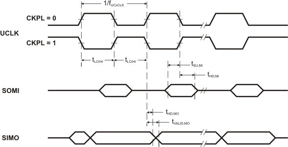 Figure 5-14 SPI Master Mode, CKPH = 0
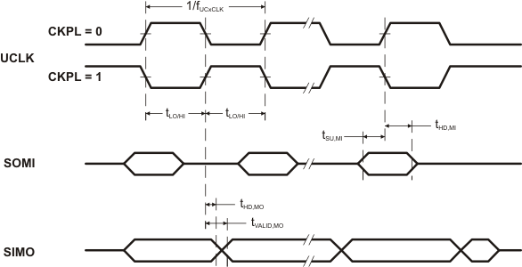 Figure 5-15 SPI Master Mode, CKPH = 1
5.29 USCI (SPI Slave Mode)
over recommended ranges of supply voltage and operating free-air temperature (unless otherwise noted)(1)(see Figure 5-16 and Figure 5-17)
| PARAMETER | TEST CONDITIONS | PMMCOREVx | VCC | MIN | MAX | UNIT | |
|---|---|---|---|---|---|---|---|
| tSTE,LEAD | STE lead time, STE low to clock | 0 | 1.8 V | 11 | ns | ||
| 3 V | 8 | ||||||
| 3 | 2.4 V | 7 | |||||
| 3 V | 6 | ||||||
| tSTE,LAG | STE lag time, Last clock to STE high | 0 | 1.8 V | 3 | ns | ||
| 3 V | 3 | ||||||
| 3 | 2.4 V | 3 | |||||
| 3 V | 3 | ||||||
| tSTE,ACC | STE access time, STE low to SOMI data out | 0 | 1.8 V | 66 | ns | ||
| 3 V | 50 | ||||||
| 3 | 2.4 V | 36 | |||||
| 3 V | 30 | ||||||
| tSTE,DIS | STE disable time, STE high to SOMI high impedance | 0 | 1.8 V | 30 | ns | ||
| 3 V | 23 | ||||||
| 3 | 2.4 V | 16 | |||||
| 3 V | 13 | ||||||
| tSU,SI | SIMO input data setup time | 0 | 1.8 V | 5 | ns | ||
| 3 V | 5 | ||||||
| 3 | 2.4 V | 2 | |||||
| 3 V | 2 | ||||||
| tHD,SI | SIMO input data hold time | 0 | 1.8 V | 5 | ns | ||
| 3 V | 5 | ||||||
| 3 | 2.4 V | 5 | |||||
| 3 V | 5 | ||||||
| tVALID,SO | SOMI output data valid time(2) | UCLK edge to SOMI valid, CL = 20 pF |
0 | 1.8 V | 76 | ns | |
| 3 V | 60 | ||||||
| 3 | 2.4 V | 44 | |||||
| 3 V | 40 | ||||||
| tHD,SO | SOMI output data hold time(3) | CL = 20 pF | 0 | 1.8 V | 18 | ns | |
| 3 V | 12 | ||||||
| 3 | 2.4 V | 10 | |||||
| 3 V | 8 | ||||||
(1) fUCxCLK = 1/2tLO/HI with tLO/HI ≥ max(tVALID,MO(Master) + tSU,SI(USCI), tSU,MI(Master) + tVALID,SO(USCI)).
For the master parameters tSU,MI(Master) and tVALID,MO(Master), see the SPI parameters of the attached master.
For the master parameters tSU,MI(Master) and tVALID,MO(Master), see the SPI parameters of the attached master.
(2) Specifies the time to drive the next valid data to the SOMI output after the output changing UCLK clock edge. See the timing diagrams in Figure 5-16 and Figure 5-17.
(3) Specifies how long data on the SOMI output is valid after the output changing UCLK clock edge. See the timing diagrams in Figure 5-16 and Figure 5-17.
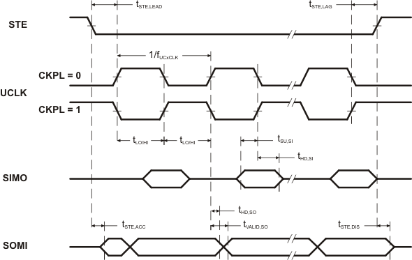 Figure 5-16 SPI Slave Mode, CKPH = 0
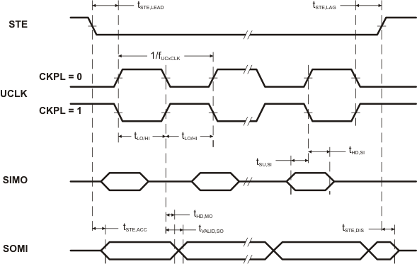 Figure 5-17 SPI Slave Mode, CKPH = 1
5.30 USCI (I2C Mode)
over recommended ranges of supply voltage and operating free-air temperature (unless otherwise noted) (see Figure 5-18)| PARAMETER | TEST CONDITIONS | VCC | MIN | MAX | UNIT | |
|---|---|---|---|---|---|---|
| fUSCI | USCI input clock frequency | Internal: SMCLK, ACLK External: UCLK Duty cycle = 50% ±10% |
fSYSTEM | MHz | ||
| fSCL | SCL clock frequency | 2.2 V, 3 V | 0 | 400 | kHz | |
| tHD,STA | Hold time (repeated) START | fSCL ≤ 100 kHz | 2.2 V, 3 V | 4.0 | µs | |
| fSCL > 100 kHz | 0.6 | |||||
| tSU,STA | Setup time for a repeated START | fSCL ≤ 100 kHz | 2.2 V, 3 V | 4.7 | µs | |
| fSCL > 100 kHz | 0.6 | |||||
| tHD,DAT | Data hold time | 2.2 V, 3 V | 0 | ns | ||
| tSU,DAT | Data setup time | 2.2 V, 3 V | 250 | ns | ||
| tSU,STO | Setup time for STOP | fSCL ≤ 100 kHz | 2.2 V, 3 V | 4.0 | µs | |
| fSCL > 100 kHz | 0.6 | |||||
| tSP | Pulse duration of spikes suppressed by input filter | 2.2 V | 50 | 600 | ns | |
| 3 V | 50 | 600 | ||||
 Figure 5-18 I2C Mode Timing
5.31 12-Bit ADC, Power Supply and Input Range Conditions
over recommended ranges of supply voltage and operating free-air temperature (unless otherwise noted)(1)| PARAMETER | TEST CONDITIONS | VCC | MIN | TYP | MAX | UNIT | |
|---|---|---|---|---|---|---|---|
| AVCC | Analog supply voltage, Full performance |
AVCC and DVCC are connected together, AVSS and DVSS are connected together, V(AVSS) = V(DVSS) = 0 V |
2.2 | 3.6 | V | ||
| V(Ax) | Analog input voltage range(2) | All ADC12 analog input pins Ax | 0 | AVCC | V | ||
| IADC12_A | Operating supply current into AVCC terminal(3) | fADC12CLK = 5.0 MHz, ADC12ON = 1, REFON = 0, SHT0 = 0, SHT1 = 0, ADC12DIV = 0 |
2.2 V | 125 | 155 | µA | |
| 3 V | 150 | 220 | |||||
| CI | Input capacitance | Only one terminal Ax can be selected at one time | 2.2 V | 20 | 25 | pF | |
| RI | Input MUX ON resistance | 0 V ≤ VAx ≤ AVCC | 10 | 200 | 1900 | Ω | |
(1) The leakage current is specified by the digital I/O input leakage.
(2) The analog input voltage range must be within the selected reference voltage range VR+ to VR– for valid conversion results. If the reference voltage is supplied by an external source or if the internal reference voltage is used and REFOUT = 1, then decoupling capacitors are required. See Section 5.35 and Section 5.36.
(3) The internal reference supply current is not included in current consumption parameter IADC12_A.
5.32 12-Bit ADC, Timing Parameters
over recommended ranges of supply voltage and operating free-air temperature (unless otherwise noted)| PARAMETER | TEST CONDITIONS | VCC | MIN | TYP | MAX | UNIT | |
|---|---|---|---|---|---|---|---|
| fADC12CLK | For specified performance of ADC12 linearity parameters | 2.2 V, 3 V | 0.45 | 4.8 | 5.4 | MHz | |
| fADC12OSC | Internal ADC12 oscillator(3) | ADC12DIV = 0, fADC12CLK = fADC12OSC | 2.2 V, 3 V | 4.2 | 4.8 | 5.4 | MHz |
| tCONVERT | Conversion time | REFON = 0, Internal oscillator, fADC12OSC = 4.2 MHz to 5.4 MHz |
2.2 V, 3 V | 2.4 | 3.1 | µs | |
| External fADC12CLK from ACLK, MCLK or SMCLK, ADC12SSEL ≠ 0 | (2) | ||||||
| tSample | Sampling time | RS = 400 Ω, RI = 1000 Ω, CI = 30 pF, τ = [RS + RI] × CI (1) |
2.2 V, 3 V | 1000 | ns | ||
(1) Approximately ten Tau (τ) are needed to get an error of less than ±0.5 LSB:
tSample = ln(2n+1) x (RS + RI) × CI + 800 ns, where n = ADC resolution = 12, RS = external source resistance
tSample = ln(2n+1) x (RS + RI) × CI + 800 ns, where n = ADC resolution = 12, RS = external source resistance
(2) 13 × ADC12DIV × 1/fADC12CLK
(3) The ADC12OSC is sourced directly from MODOSC inside the UCS.
5.33 12-Bit ADC, Linearity Parameters
over recommended ranges of supply voltage and operating free-air temperature (unless otherwise noted)| PARAMETER | TEST CONDITIONS | VCC | MIN | TYP | MAX | UNIT | |
|---|---|---|---|---|---|---|---|
| EI | Integral linearity error (INL) | 1.4 V ≤ (VeREF+ – VREF–/VeREF–)min ≤ 1.6 V | 2.2 V, 3 V | ±2 | LSB | ||
| 1.6 V < (VeREF+ – VREF–/VeREF–)min ≤ VAVCC | ±1.7 | ||||||
| ED | Differential linearity error (DNL) | (VeREF+ – VREF–/VeREF–)min ≤ (VeREF+ – VREF–/VeREF–), CVREF+ = 20 pF |
2.2 V, 3 V | ±1.0 | LSB | ||
| EO | Offset error | (VeREF+ – VREF–/VeREF–)min ≤ (VeREF+ – VREF–/VeREF–), Internal impedance of source RS < 100 Ω, CVREF+ = 20 pF |
2.2 V, 3 V | ±1.0 | ±2.0 | LSB | |
| EG | Gain error | (VeREF+ – VREF–/VeREF–)min ≤ (VeREF+ – VREF–/VeREF–), CVREF+ = 20 pF |
2.2 V, 3 V | ±1.0 | ±2.0 | LSB | |
| ET | Total unadjusted error | (VeREF+ – VREF–/VeREF–)min ≤ (VeREF+ – VREF–/VeREF–), CVREF+ = 20 pF |
2.2 V, 3 V | ±1.4 | ±3.5 | LSB | |
5.34 12-Bit ADC, Temperature Sensor and Built-In VMID (1)
over recommended ranges of supply voltage and operating free-air temperature (unless otherwise noted)| PARAMETER | TEST CONDITIONS | VCC | MIN | TYP | MAX | UNIT | |
|---|---|---|---|---|---|---|---|
| VSENSOR | See (2) (3) | ADC12ON = 1, INCH = 0Ah, TA = 0°C |
2.2 V | 680 | mV | ||
| 3 V | 680 | ||||||
| TCSENSOR | See (3) | ADC12ON = 1, INCH = 0Ah | 2.2 V | 2.25 | mV/°C | ||
| 3 V | 2.25 | ||||||
| tSENSOR(sample) | Sample time required if channel 10 is selected(4) | ADC12ON = 1, INCH = 0Ah, Error of conversion result ≤1 LSB |
2.2 V | 100 | µs | ||
| 3 V | 100 | ||||||
| VMID | AVCC divider at channel 11, VAVCC factor | ADC12ON = 1, INCH = 0Bh | 0.48 | 0.5 | 0.52 | VAVCC | |
| AVCC divider at channel 11 | ADC12ON = 1, INCH = 0Bh | 2.2 V | 1.06 | 1.1 | 1.14 | V | |
| 3 V | 1.44 | 1.5 | 1.56 | ||||
| tVMID(sample) | Sample time required if channel 11 is selected(5) | ADC12ON = 1, INCH = 0Bh, Error of conversion result ≤1 LSB |
2.2 V, 3 V | 1000 | ns | ||
(1) The temperature sensor is provided by the REF module. See the REF module parametric, IREF+, regarding the current consumption of the temperature sensor.
(2) The temperature sensor offset can be significant. TI recommends a single-point calibration to minimize the offset error of the built-in temperature sensor.
(3) The device descriptor structure contains calibration values for 30°C ±3°C and 85°C ±3°C for each of the available reference voltage levels. The sensor voltage can be computed as VSENSE = TCSENSOR * (Temperature, °C) + VSENSOR, where TCSENSOR and VSENSOR can be computed from the calibration values for higher accuracy.
(4) The typical equivalent impedance of the sensor is 51 kΩ. The sample time required includes the sensor-on time tSENSOR(on).
(5) The on-time tVMID(on) is included in the sampling time tVMID(sample); no additional on time is needed.
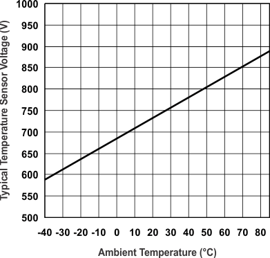 Figure 5-19 Typical Temperature Sensor Voltage
5.35 REF, External Reference
over recommended ranges of supply voltage and operating free-air temperature (unless otherwise noted)(1)| PARAMETER | TEST CONDITIONS | VCC | MIN | TYP | MAX | UNIT | |
|---|---|---|---|---|---|---|---|
| VeREF+ | Positive external reference voltage input | VeREF+ > VREF–/VeREF– (2) | 1.4 | AVCC | V | ||
| VREF–/VeREF– | Negative external reference voltage input | VeREF+ > VREF–/VeREF– (3) | 0 | 1.2 | V | ||
| (VeREF+ – VREF–/VeREF–) |
Differential external reference voltage input | VeREF+ > VREF–/VeREF– (4) | 1.4 | AVCC | V | ||
| IVeREF+
IVREF-/VeREF– |
Static input current | 1.4 V ≤ VeREF+ ≤ VAVCC, VeREF– = 0 V, fADC12CLK = 5 MHz, ADC12SHTx = 1h, Conversion rate 200ksps |
2.2 V, 3 V | ±8.5 | ±26 | µA | |
| 1.4 V ≤ VeREF+ ≤ VAVCC, VeREF– = 0 V fADC12CLK = 5 MHz, ADC12SHTx = 8h, Conversion rate 20 ksps |
2.2 V, 3 V | ±1 | |||||
| CVREF± | Capacitance at VREF+ or VREF- terminal, external reference(5) | 10 | µF | ||||
(1) The external reference is used during ADC conversion to charge and discharge the capacitance array. The input capacitance, Ci, is also the dynamic load for an external reference during conversion. The dynamic impedance of the reference supply should follow the recommendations on analog-source impedance to allow the charge to settle for 12-bit accuracy.
(2) The accuracy limits the minimum positive external reference voltage. Lower reference voltage levels may be applied with reduced accuracy requirements.
(3) The accuracy limits the maximum negative external reference voltage. Higher reference voltage levels may be applied with reduced accuracy requirements.
(4) The accuracy limits minimum external differential reference voltage. Lower differential reference voltage levels may be applied with reduced accuracy requirements.
(5) Two decoupling capacitors, 10 µF and 100 nF, should be connected to VREF to decouple the dynamic current required for an external reference source if it is used for the ADC12_A. See also the RF430F5978 User's Guide (SLAU378).
5.36 REF, Built-In Reference
over recommended ranges of supply voltage and operating free-air temperature (unless otherwise noted)(1)| PARAMETER | TEST CONDITIONS | VCC | MIN | TYP | MAX | UNIT | |
|---|---|---|---|---|---|---|---|
| VREF+ | Positive built-in reference voltage output | REFVSEL = 2 for 2.5 V, REFON = REFOUT = 1, IVREF+ = 0 A |
3 V | 2.41 | ±1.5% | V | |
| REFVSEL = 1 for 2 V, REFON = REFOUT = 1, IVREF+ = 0 A |
3 V | 1.93 | ±1.5% | ||||
| REFVSEL = 0 for 1.5 V, REFON = REFOUT = 1, IVREF+ = 0 A |
2.2 V, 3 V | 1.45 | ±1.5% | ||||
| AVCC(min) | AVCC minimum voltage, Positive built-in reference active | REFVSEL = 0 for 1.5 V, reduced performance | 1.8 | V | |||
| REFVSEL = 0 for 1.5 V | 2.2 | ||||||
| REFVSEL = 1 for 2 V | 2.3 | ||||||
| REFVSEL = 2 for 2.5 V | 2.8 | ||||||
| IREF+ | Operating supply current into AVCC terminal(2) (3) | REFON = 1, REFOUT = 0, REFBURST = 0 | 3 V | 100 | 140 | µA | |
| REFON = 1, REFOUT = 1, REFBURST = 0 | 3 V | 0.9 | 1.5 | mA | |||
| IL(VREF+) | Load-current regulation, VREF+ terminal(4) | REFVSEL = (0, 1, or 2), IVREF+ = +10 µA/–1000 µA, AVCC = AVCC (min) for each reference level, REFVSEL = (0, 1, or 2), REFON = REFOUT = 1 |
2500 | µV/mA | |||
| CVREF± | Capacitance at VREF+ and VREF- terminals, internal reference | REFON = REFOUT = 1 | 20 | 100 | pF | ||
| TCREF+ | Temperature coefficient of built-in reference(5) | IVREF+ = 0 A, REFVSEL = (0, 1, or 2), REFON = 1, REFOUT = 0 or 1 |
30 | 50 | ppm/ °C | ||
| PSRR_DC | Power supply rejection ratio (DC) | AVCC = AVCC (min) to AVCC(max), TA = 25°C, REFVSEL = (0, 1, or 2), REFON = 1, REFOUT = 0 or 1 |
120 | 300 | µV/V | ||
| PSRR_AC | Power supply rejection ratio (AC) | AVCC = AVCC (min) to AVCC(max)
TA = 25°C, f = 1 kHz, ΔVpp = 100 mV, REFVSEL = 0, 1, or 2, REFON = 1, REFOUT = 0 or 1 |
6.4 | mV/V | |||
| tSETTLE | Settling time of reference voltage(6) | AVCC = AVCC (min) to AVCC(max), REFVSEL = (0, 1, or 2), REFOUT = 0, REFON = 0 → 1 |
75 | µs | |||
| AVCC = AVCC (min) to AVCC(max), CVREF = CVREF(max), REFVSEL = (0, 1, or 2), REFOUT = 1, REFON = 0 → 1 |
75 | ||||||
(1) The reference is supplied to the ADC by the REF module and is buffered locally inside the ADC. The ADC uses two internal buffers, one smaller and one larger for driving the VREF+ terminal. When REFOUT = 1, the reference is available at the VREF+ terminal, as well as, used as the reference for the conversion and utilizes the larger buffer. When REFOUT = 0, the reference is only used as the reference for the conversion and utilizes the smaller buffer.
(2) The internal reference current is supplied through the AVCC terminal. Consumption is independent of the ADC12ON control bit, unless a conversion is active. The REFON bit enables to settle the built-in reference before starting an A/D conversion. REFOUT = 0 represents the current contribution of the smaller buffer. REFOUT = 1 represents the current contribution of the larger buffer without external load.
(3) The temperature sensor is provided by the REF module. Its current is supplied through the AVCC terminal and is equivalent to IREF+ with REFON = 1 and REFOUT = 0.
(4) Contribution only due to the reference and buffer including package. This does not include resistance due to PCB trace, etc.
(5) Calculated using the box method: (MAX(–40°C to 85°C) – MIN(–40°C to 85°C)) / MIN(–40°C to 85°C)/(85°C – (–40°C)).
(6) The condition is that the error in a conversion started after tREFON is less than ±0.5 LSB. The settling time depends on the external capacitive load when REFOUT = 1.
5.37 Comparator B
over recommended ranges of supply voltage and operating free-air temperature (unless otherwise noted)| PARAMETER | TEST CONDITIONS | VCC | MIN | TYP | MAX | UNIT | |
|---|---|---|---|---|---|---|---|
| VCC | Supply voltage | 1.8 | 3.6 | V | |||
| IAVCC_COMP | Comparator operating supply current into AVCC, Excludes reference resistor ladder | CBPWRMD = 00 | 1.8 V | 40 | µA | ||
| 2.2 V | 30 | 50 | |||||
| 3 V | 40 | 65 | |||||
| CBPWRMD = 01 | 2.2 V, 3 V | 10 | 30 | ||||
| CBPWRMD = 10 | 2.2 V, 3 V | 0.1 | 0.5 | ||||
| IAVCC_REF | Quiescent current of local reference voltage amplifier into AVCC | CBREFACC = 1, CBREFLx = 01 | 22 | µA | |||
| VIC | Common mode input range | 0 | VCC–1 | V | |||
| VOFFSET | Input offset voltage | CBPWRMD = 00 | ±20 | mV | |||
| CBPWRMD = 01, 10 | ±10 | ||||||
| CIN | Input capacitance | 5 | pF | ||||
| RSIN | Series input resistance | ON - switch closed | 3 | 4 | kΩ | ||
| OFF - switch opened | 30 | MΩ | |||||
| tPD | Propagation delay, response time | CBPWRMD = 00, CBF = 0 | 450 | ns | |||
| CBPWRMD = 01, CBF = 0 | 600 | ||||||
| CBPWRMD = 10, CBF = 0 | 50 | µs | |||||
| tPD,filter | Propagation delay with filter active | CBPWRMD = 00, CBON = 1, CBF = 1, CBFDLY = 00 |
0.35 | 0.6 | 1.0 | µs | |
| CBPWRMD = 00, CBON = 1, CBF = 1, CBFDLY = 01 |
0.6 | 1.0 | 1.8 | ||||
| CBPWRMD = 00, CBON = 1, CBF = 1, CBFDLY = 10 |
1.0 | 1.8 | 3.4 | ||||
| CBPWRMD = 00, CBON = 1, CBF = 1, CBFDLY = 11 |
1.8 | 3.4 | 6.5 | ||||
| tEN_CMP | Comparator enable time, settling time | CBON = 0 to CBON = 1, CBPWRMD = 00, 01, 10 |
1 | 2 | µs | ||
| tEN_REF | Resistor reference enable time | CBON = 0 to CBON = 1 | 0.3 | 1.5 | µs | ||
| VCB_REF | Reference voltage for a given tap | VIN = reference into resistor ladder, n = 0 to 31 |
VIN × (n + 1) / 32 | V | |||
5.38 Flash Memory
over recommended ranges of supply voltage and operating free-air temperature (unless otherwise noted)| PARAMETER | TJ | MIN | TYP | MAX | UNIT | |
|---|---|---|---|---|---|---|
| DVCC(PGM/ERASE) | Program and erase supply voltage | 1.8 | 3.6 | V | ||
| IPGM | Average supply current from DVCC during program | 3 | 5 | mA | ||
| IERASE | Average supply current from DVCC during erase | 2 | 6.5 | mA | ||
| IMERASE, IBANK | Average supply current from DVCC during mass erase or bank erase | 2 | 6.5 | mA | ||
| tCPT | Cumulative program time(1) | 16 | ms | |||
| Program and erase endurance | 104 | 105 | cycles | |||
| tRetention | Data retention duration | 25°C | 100 | years | ||
| tWord | Word or byte program time(2) | 64 | 85 | µs | ||
| tBlock, 0 | Block program time for first byte or word(2) | 49 | 65 | µs | ||
| tBlock, 1–(N–1) | Block program time for each additional byte or word, except for last byte or word(2) | 37 | 49 | µs | ||
| tBlock, N | Block program time for last byte or word(2) | 55 | 73 | µs | ||
| tErase | Erase time for segment erase, mass erase, and bank erase when available(2) | 23 | 32 | ms | ||
| fMCLK,MRG | MCLK frequency in marginal read mode (FCTL4.MRG0 = 1 or FCTL4. MRG1 = 1) |
0 | 1 | MHz | ||
(1) The cumulative program time must not be exceeded when writing to a 128-byte flash block. This parameter applies to all programming methods: individual word or byte write and block write modes.
(2) These values are hardwired into the state machine of the flash controller.
5.39 JTAG and Spy-Bi-Wire Interface
over recommended ranges of supply voltage and operating free-air temperature (unless otherwise noted)| PARAMETER | VCC | MIN | TYP | MAX | UNIT | |
|---|---|---|---|---|---|---|
| fSBW | Spy-Bi-Wire input frequency | 2.2 V, 3 V | 0 | 20 | MHz | |
| tSBW,Low | Spy-Bi-Wire low clock pulse duration | 2.2 V, 3 V | 0.025 | 15 | µs | |
| tSBW, En | Spy-Bi-Wire enable time (TEST high to acceptance of first clock edge)(1) | 2.2 V, 3 V | 1 | µs | ||
| tSBW,Rst | Spy-Bi-Wire return to normal operation time | 15 | 100 | µs | ||
| fTCK | TCK input frequency to 4-wire JTAG(2) | 2.2 V | 0 | 5 | MHz | |
| 3 V | 0 | 10 | MHz | |||
| Rinternal | Internal pulldown resistance on TEST | 2.2 V, 3 V | 45 | 60 | 80 | kΩ |
(1) Tools that access the Spy-Bi-Wire interface must wait for the minimum tSBW,En time after pulling the TEST/SBWTCK pin high before applying the first SBWTCK clock edge.
(2) fTCK may be restricted to meet the timing requirements of the module selected.
5.40 RF1A CC1101 Radio Parameters
Table 5-1 Recommended Operating Conditions
| MIN | NOM | MAX | UNIT | ||
|---|---|---|---|---|---|
| VCC | Supply voltage range during radio operation | 2.0 | 3.6 | V | |
| PMMCOREVx | Core voltage range, PMMCOREVx setting during radio operation | 2 | 3 | ||
| RF frequency range | 300 | 348 | MHz | ||
| 389(1) | 464 | ||||
| 779 | 928 | ||||
| Data rate | 2-FSK | 0.6 | 500 | kBaud | |
| 2-GFSK, OOK, and ASK | 0.6 | 250 | |||
| (Shaped) MSK (also known as differential offset QPSK)(2) | 26 | 500 | |||
| RF crystal frequency | 26 | 26 | 27 | MHz | |
| RF crystal tolerance | Total tolerance including initial tolerance, crystal loading, aging and temperature dependency.(3) | ±40 | ppm | ||
| RF crystal load capacitance | 10 | 13 | 20 | pF | |
| RF crystal effective series resistance | 100 | Ω | |||
(1) If using a 27-MHz crystal, the lower frequency limit for this band is 392 MHz.
(2) If using optional Manchester encoding, the data rate in kbps is half the baud rate.
(3) The acceptable crystal tolerance depends on frequency band, channel bandwidth, and spacing. Also see design note DN005 -- CC11xx Sensitivity versus Frequency Offset and Crystal Accuracy (SWRA122).
5.40.1 RF Crystal Oscillator, XT2
TA = 25°C, VCC = 3 V (unless otherwise noted)(1)| PARAMETER | MIN | TYP | MAX | UNIT | |
|---|---|---|---|---|---|
| Start-up time(1) | 150 | 810 | µs | ||
| Duty cycle | 45% | 50% | 55% | ||
(1) The start-up time depends to a very large degree on the crystal that is used.
5.40.2 Current Consumption, Reduced-Power Modes
TA = 25°C, VCC = 3 V (unless otherwise noted)(1)| PARAMETER | TEST CONDITIONS | MIN | TYP | MAX | UNIT | |
|---|---|---|---|---|---|---|
| Current consumption | RF crystal oscillator only(3) | 100 | µA | |||
| IDLE state (including RF crystal oscillator) | 1.7 | mA | ||||
| FSTXON state (only the frequency synthesizer is running)(2) | 9.5 | mA | ||||
(1) All measurement results are obtained using the EM430F6137RF900 with BOM according to tested frequency range.
(2) This current consumption is also representative of other intermediate states when going from IDLE to RX or TX, including the calibration state.
(3) To measure the current, follow this sequence:
- Enable XT2 with XOSC_FORCE_ON = 1.
- Set radio to sleep mode.
- Disable XT2 clock requests from any module.
5.40.3 Current Consumption, Receive Mode
TA = 25°C, VCC = 3 V (unless otherwise noted)(1) (1)| PARAMETER | FREQ (MHz) | DATA RATE (kBaud) | TEST CONDITIONS | MIN | TYP | MAX | UNIT | |
|---|---|---|---|---|---|---|---|---|
| Current consumption, RX | 315 | 1.2 | Register settings optimized for reduced current | Input at –100 dBm (close to sensitivity limit) | 17 | mA | ||
| Input at –40 dBm (well above sensitivity limit) | 16 | |||||||
| 38.4 | Input at –100 dBm (close to sensitivity limit) | 17 | ||||||
| Input at –40 dBm (well above sensitivity limit) | 16 | |||||||
| 250 | Input at –100 dBm (close to sensitivity limit) | 18 | ||||||
| Input at –40 dBm (well above sensitivity limit) | 16.5 | |||||||
| 433 | 1.2 | Register settings optimized for reduced current | Input at –100 dBm (close to sensitivity limit) | 18 | ||||
| Input at –40 dBm (well above sensitivity limit) | 17 | |||||||
| 38.4 | Input at –100 dBm (close to sensitivity limit) | 18 | ||||||
| Input at –40 dBm (well above sensitivity limit) | 17 | |||||||
| 250 | Input at –100 dBm (close to sensitivity limit) | 18.5 | ||||||
| Input at –40 dBm (well above sensitivity limit) | 17 | |||||||
| 868, 915 | 1.2 | Register settings optimized for reduced current(2) | Input at –100 dBm (close to sensitivity limit) | 16 | ||||
| Input at –40 dBm (well above sensitivity limit) | 15 | |||||||
| 38.4 | Input at –100 dBm (close to sensitivity limit) | 16 | ||||||
| Input at –40 dBm (well above sensitivity limit) | 15 | |||||||
| 250 | Input at –100 dBm (close to sensitivity limit) | 16 | ||||||
| Input at –40 dBm (well above sensitivity limit) | 15 | |||||||
(1) Reduced current setting (MDMCFG2.DEM_DCFILT_OFF = 1) gives a slightly lower current consumption at the cost of a reduction in sensitivity. See tables "RF Receive" for additional details on current consumption and sensitivity.
(2) For 868 or 915 MHz, see Figure 5-20 for current consumption with register settings optimized for sensitivity.
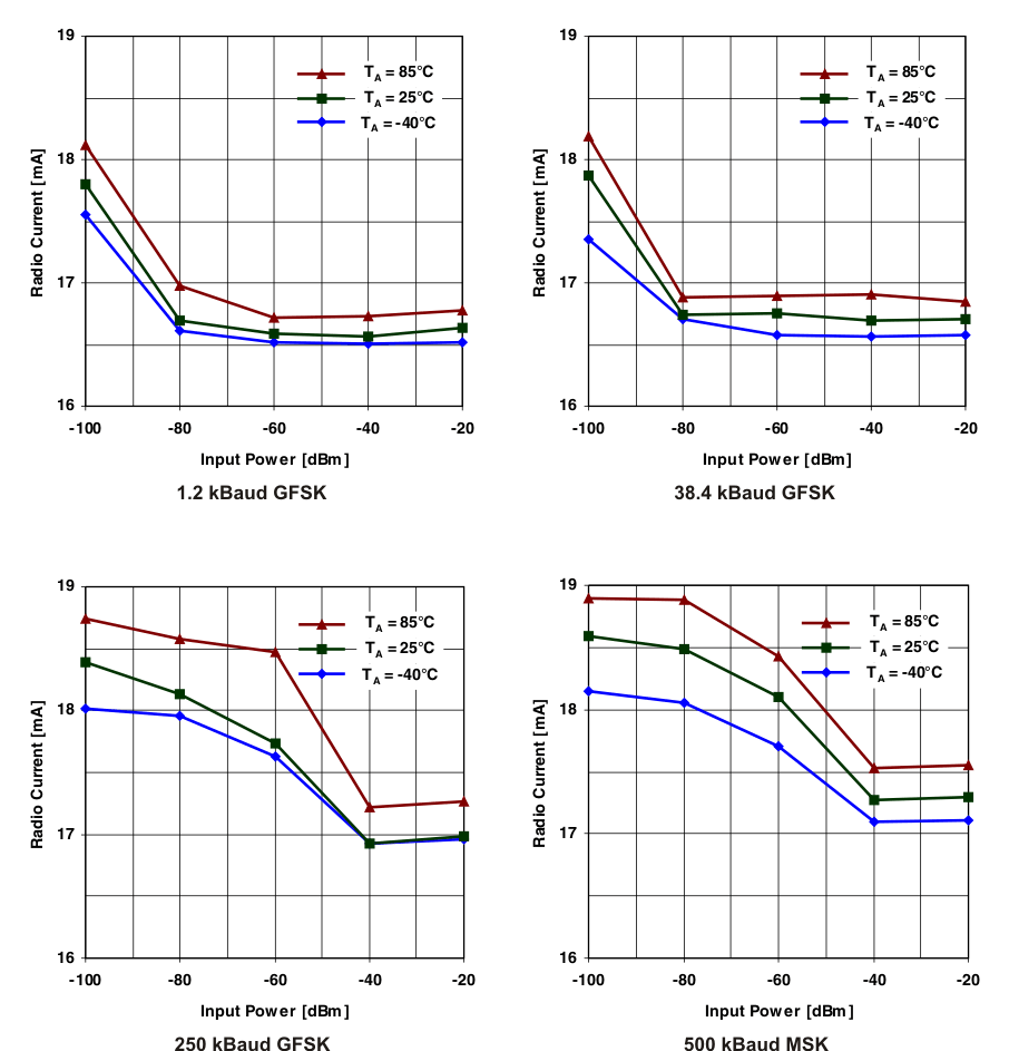 Figure 5-20 Typical RX Current Consumption Over Temperature and Input Power Level, 868 MHz, Sensitivity-Optimized Setting
5.40.4 Current Consumption, Transmit Mode
TA = 25°C, VCC = 3 V (unless otherwise noted)(1) (1)| PARAMETER | FREQUENCY [MHz} | PATABLE SETTING | OUTPUT POWER (dBm) | TYP | UNIT |
|---|---|---|---|---|---|
| Current consumption, TX | 315 | 0xC0 | Maximum | 26 | mA |
| 0xC4 | +10 | 25 | |||
| 0x51 | 0 | 15 | |||
| 0x29 | –6 | 15 | |||
| 433 | 0xC0 | Maximum | 33 | ||
| 0xC6 | +10 | 29 | |||
| 0x50 | 0 | 17 | |||
| 0x2D | –6 | 17 | |||
| 868 | 0xC0 | Maximum | 36 | ||
| 0xC3 | +10 | 33 | |||
| 0x8D | 0 | 18 | |||
| 0x2D | –6 | 18 | |||
| 915 | 0xC0 | Maximum | 35 | ||
| 0xC3 | +10 | 32 | |||
| 0x8D | 0 | 18 | |||
| 0x2D | –6 | 18 |
5.40.5 Typical TX Current Consumption, 315 MHz
| PARAMETER | PATABLE SETTING | OUTPUT POWER (dBm) | VCC | 2 V | 3 V | 3.6 V | UNIT | ||||||
|---|---|---|---|---|---|---|---|---|---|---|---|---|---|
| TA | 25°C | 25°C | 25°C | ||||||||||
| Current consumption, TX | 0xC0 | Maximum | 27.5 | 26.4 | 28.1 | mA | |||||||
| 0xC4 | +10 | 25.1 | 25.2 | 25.3 | |||||||||
| 0x51 | 0 | 14.4 | 14.6 | 14.7 | |||||||||
| 0x29 | –6 | 14.2 | 14.7 | 15.0 | |||||||||
5.40.6 Typical TX Current Consumption, 433 MHz
| PARAMETER | PATABLE SETTING | OUTPUT POWER (dBm) | VCC | 2 V | 3 V | 3.6 V | UNIT | ||||||
|---|---|---|---|---|---|---|---|---|---|---|---|---|---|
| TA | 25°C | 25°C | 25°C | ||||||||||
| Current consumption, TX | 0xC0 | Maximum | 33.1 | 33.4 | 33.8 | mA | |||||||
| 0xC6 | +10 | 28.6 | 28.8 | 28.8 | |||||||||
| 0x50 | 0 | 16.6 | 16.8 | 16.9 | |||||||||
| 0x2D | –6 | 16.8 | 17.5 | 17.8 | |||||||||
5.40.7 Typical TX Current Consumption, 868 MHz
| PARAMETER | PATABLE SETTING | OUTPUT POWER (dBm) | VCC | 2 V | 3 V | 3.6 V | UNIT | ||||||
|---|---|---|---|---|---|---|---|---|---|---|---|---|---|
| TA | –40°C | 25°C | 85°C | –40°C | 25°C | 85°C | –40°C | 25°C | 85°C | ||||
| Current consumption, TX | 0xC0 | Maximum | 36.7 | 35.2 | 34.2 | 38.5 | 35.5 | 34.9 | 37.1 | 35.7 | 34.7 | mA | |
| 0xC3 | +10 | 34.0 | 32.8 | 32.0 | 34.2 | 33.0 | 32.5 | 34.3 | 33.1 | 32.2 | |||
| 0x8D | 0 | 18.0 | 17.6 | 17.5 | 18.3 | 17.8 | 18.1 | 18.4 | 18.0 | 17.7 | |||
| 0x2D | –6 | 17.1 | 17.0 | 17.2 | 17.8 | 17.8 | 18.3 | 18.2 | 18.1 | 18.1 | |||
5.40.8 Typical TX Current Consumption, 915 MHz
| PARAMETER | PATABLE SETTING | OUTPUT POWER (dBm) | VCC | 2 V | 3 V | 3.6 V | UNIT | ||||||
|---|---|---|---|---|---|---|---|---|---|---|---|---|---|
| TA | –40°C | 25°C | 85°C | –40°C | 25°C | 85°C | –40°C | 25°C | 85°C | ||||
| Current consumption, TX | 0xC0 | Maximum | 35.5 | 33.8 | 33.2 | 36.2 | 34.8 | 33.6 | 36.3 | 35.0 | 33.8 | mA | |
| 0xC3 | +10 | 33.2 | 32.0 | 31.0 | 33.4 | 32.1 | 31.2 | 33.5 | 32.3 | 31.3 | |||
| 0x8D | 0 | 17.8 | 17.4 | 17.1 | 18.1 | 17.6 | 17.3 | 18.2 | 17.8 | 17.5 | |||
| 0x2D | –6 | 17.0 | 16.9 | 16.9 | 17.7 | 17.6 | 17.6 | 18.1 | 18.0 | 18.0 | |||
5.40.9 RF Receive, Overall
TA = 25°C, VCC = 3 V (unless otherwise noted)(1)| PARAMETER | TEST CONDITIONS | MIN | TYP | MAX | UNIT |
|---|---|---|---|---|---|
| Digital channel filter bandwidth(1) | 58 | 812 | kHz | ||
| Spurious emissions(3) (2) | 25 MHz to 1 GHz | –68 | –57 | dBm | |
| Above 1 GHz | –66 | –47 | |||
| RX latency | Serial operation(4) | 9 | bit |
(1) User programmable. The bandwidth limits are proportional to crystal frequency (given values assume a 26.0-MHz crystal).
(2) Maximum figure is the ETSI EN 300 220 limit
(3) Typical radiated spurious emission is –49 dBm measured at the VCO frequency
(4) Time from start of reception until data is available on the receiver data output pin is equal to 9 bit.
5.40.10 RF Receive, 315 MHz
TA = 25°C, VCC = 3 V (unless otherwise noted)(1)2-FSK, 1% packet error rate, 20-byte packet length, Sensitivity optimized, MDMCFG2.DEM_DCFILT_OFF = 0 (unless otherwise noted)
| PARAMETER | DATA RATE (kBaud) | TEST CONDITIONS | TYP | UNIT |
|---|---|---|---|---|
| Receiver sensitivity | 0.6 | 14.3-kHz deviation, 58-kHz digital channel filter bandwidth | –117 | dBm |
| 1.2 | 5.2-kHz deviation, 58-kHz digital channel filter bandwidth(1) | –111 | ||
| 38.4 | 20-kHz deviation, 100-kHz digital channel filter bandwidth(2) | –103 | ||
| 250 | 127-kHz deviation, 540-kHz digital channel filter bandwidth (3) | –95 | ||
| 500 | MSK, 812-kHz digital channel filter bandwidth(3) | –86 |
(1) Sensitivity can be traded for current consumption by setting MDMCFG2.DEM_DCFILT_OFF = 1. The typical current consumption is then reduced by approximately 2 mA close to the sensitivity limit. The sensitivity is typically reduced to –109 dBm.
(2) Sensitivity can be traded for current consumption by setting MDMCFG2.DEM_DCFILT_OFF = 1. The typical current consumption is then reduced by approximately 2 mA close to the sensitivity limit. The sensitivity is typically reduced to –102 dBm.
(3) MDMCFG2.DEM_DCFILT_OFF = 1 can not be used for data rates ≥ 250 kBaud.
5.40.11 RF Receive, 433 MHz
TA = 25°C, VCC = 3 V (unless otherwise noted)(1)2-FSK, 1% packet error rate, 20-byte packet length, Sensitivity optimized, MDMCFG2.DEM_DCFILT_OFF = 0 (unless otherwise noted)
| PARAMETER | DATA RATE (kBaud) | TEST CONDITIONS | MIN | TYP | MAX | UNIT |
|---|---|---|---|---|---|---|
| Receiver sensitivity | 0.6 | 14.3-kHz deviation, 58-kHz digital channel filter bandwidth | –114 | dBm | ||
| 1.2 | 5.2-kHz deviation, 58-kHz digital channel filter bandwidth(1) | –111 | ||||
| 38.4 | 20-kHz deviation, 100-kHz digital channel filter bandwidth(2) | –104 | ||||
| 250 | 127-kHz deviation, 540-kHz digital channel filter bandwidth (3) | –93 | ||||
| 500 | MSK, 812-kHz digital channel filter bandwidth(3) | –85 |
(1) Sensitivity can be traded for current consumption by setting MDMCFG2.DEM_DCFILT_OFF = 1. The typical current consumption is then reduced by approximately 2 mA close to the sensitivity limit. The sensitivity is typically reduced to –109 dBm.
(2) Sensitivity can be traded for current consumption by setting MDMCFG2.DEM_DCFILT_OFF = 1. The typical current consumption is then reduced by approximately 2 mA close to the sensitivity limit. The sensitivity is typically reduced to –101 dBm.
5.40.12 RF Receive, 868 or 915 MHz
TA = 25°C, VCC = 3 V (unless otherwise noted)(1),1% packet error rate, 20-byte packet length, Sensitivity optimized, MDMCFG2.DEM_DCFILT_OFF = 0 (unless otherwise noted)
| PARAMETER | TEST CONDITIONS | MIN | TYP | MAX | UNIT | |
|---|---|---|---|---|---|---|
| 0.6-kBaud data rate, 2-FSK, 14.3-kHz deviation, 58-kHz digital channel filter bandwidth (unless otherwise noted) | ||||||
| Receiver sensitivity | –115 | dBm | ||||
| 1.2-kBaud data rate, 2-FSK, 5.2-kHz deviation, 58-kHz digital channel filter bandwidth (unless otherwise noted) | ||||||
| Receiver sensitivity(1) | –109 | dBm | ||||
| 2-GFSK modulation by setting MDMCFG2.MOD_FORMAT = 2, Gaussian filter with BT = 0.5 |
–109 | |||||
| Saturation | FIFOTHR.CLOSE_IN_RX = 0(3) | –28 | dBm | |||
| Adjacent channel rejection | Desired channel 3 dB above the sensitivity limit, 100-kHz channel spacing(2) | –100-kHz offset | 39 | dB | ||
| +100-kHz offset | 39 | |||||
| Image channel rejection | IF frequency 152 kHz, desired channel 3 dB above the sensitivity limit | 29 | dB | |||
| Blocking | Desired channel 3 dB above the sensitivity limit(4) | ±2-MHz offset | –48 | dBm | ||
| ±10-MHz offset | –40 | |||||
| 38.4-kBaud data rate, 2-FSK, 20-kHz deviation, 100-kHz digital channel filter bandwidth (unless otherwise noted) | ||||||
| Receiver sensitivity(5) | –102 | dBm | ||||
| 2-GFSK modulation by setting MDMCFG2.MOD_FORMAT = 2, Gaussian filter with BT = 0.5 |
–101 | |||||
| Saturation | FIFOTHR.CLOSE_IN_RX = 0(3) | –19 | dBm | |||
| Adjacent channel rejection | Desired channel 3 dB above the sensitivity limit, 200 kHz channel spacing(4) | –200-kHz offset | 20 | dB | ||
| +200-kHz offset | 25 | |||||
| Image channel rejection | IF frequency 152 kHz, Desired channel 3 dB above the sensitivity limit | 23 | dB | |||
| Blocking | Desired channel 3 dB above the sensitivity limit(4) | ±2-MHz offset | –48 | dBm | ||
| ±10-MHz offset | –40 | |||||
| 250-kBaud data rate, 2-FSK, 127-kHz deviation, 540-kHz digital channel filter bandwidth (unless otherwise noted) | ||||||
| Receiver sensitivity (7) | –90 | dBm | ||||
| 2-GFSK modulation by setting MDMCFG2.MOD_FORMAT = 2, Gaussian filter with BT = 0.5 |
–90 | |||||
| Saturation | FIFOTHR.CLOSE_IN_RX = 0(3) | –19 | dBm | |||
| Adjacent channel rejection | Desired channel 3 dB above the sensitivity limit, 750-kHz channel spacing(6) | –750-kHz offset | 24 | dB | ||
| +750-kHz offset | 30 | |||||
| Image channel rejection | IF frequency 304 kHz, Desired channel 3 dB above the sensitivity limit | 18 | dB | |||
| Blocking | Desired channel 3 dB above the sensitivity limit(6) | ±2-MHz offset | –53 | dBm | ||
| ±10-MHz offset | –39 | |||||
| 500-kBaud data rate, MSK, 812-kHz digital channel filter bandwidth (unless otherwise noted) | ||||||
| Receiver sensitivity(7) | –84 | dBm | ||||
| Image channel rejection | IF frequency 355 kHz, Desired channel 3 dB above the sensitivity limit | –2 | dB | |||
| Blocking | Desired channel 3 dB above the sensitivity limit(8) | ±2-MHz offset | –53 | dBm | ||
| ±10-MHz offset | –38 | |||||
(1) Sensitivity can be traded for current consumption by setting MDMCFG2.DEM_DCFILT_OFF = 1. The typical current consumption is then reduced by approximately 2 mA close to the sensitivity limit. The sensitivity is typically reduced to –107 dBm.
(2) See Figure 5-21 for blocking performance at other offset frequencies.
(3) See design note DN010 Close-in Reception with CC1101 (SWRA147).
(4) See Figure 5-22 for blocking performance at other offset frequencies.
(5) Sensitivity can be traded for current consumption by setting MDMCFG2.DEM_DCFILT_OFF = 1. The typical current consumption is then reduced by approximately 2 mA close to the sensitivity limit. The sensitivity is typically reduced to –100 dBm.
(6) See Figure 5-23 for blocking performance at other offset frequencies.
(7) MDMCFG2.DEM_DCFILT_OFF = 1 cannot be used for data rates ≥ 250 kBaud.
(8) See Figure 5-24 for blocking performance at other offset frequencies.
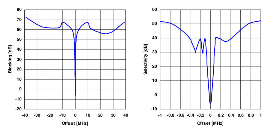
A.
Figure 5-21 Typical Selectivity at 1.2-kBaud Data Rate
NOTE:
868.3 MHz, 2-FSK, 5.2-kHz deviation, IF frequency is 152.3 kHz, digital channel filter bandwidth is 58 kHz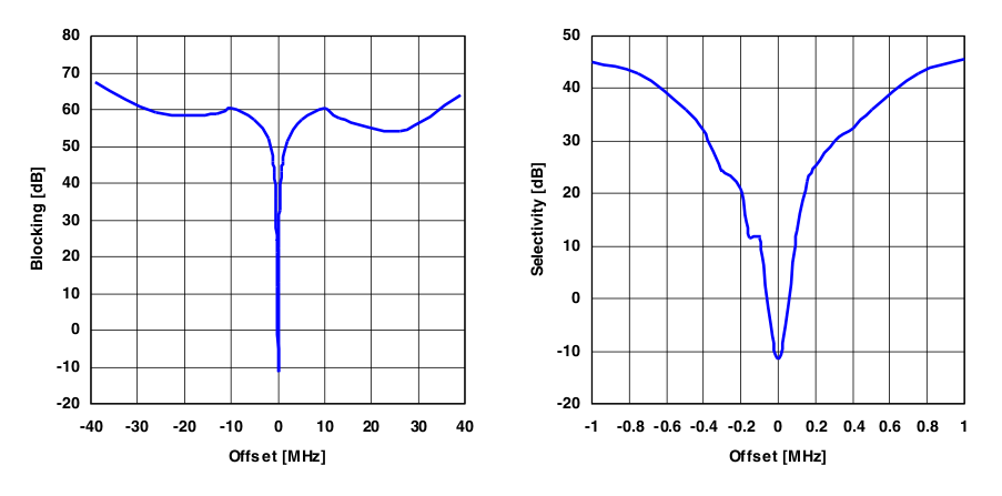
A.
Figure 5-22 Typical Selectivity at 38.4-kBaud Data Rate
NOTE:
868 MHz, 2-FSK, 20 kHz deviation, IF frequency is 152.3 kHz, digital channel filter bandwidth is 100 kHz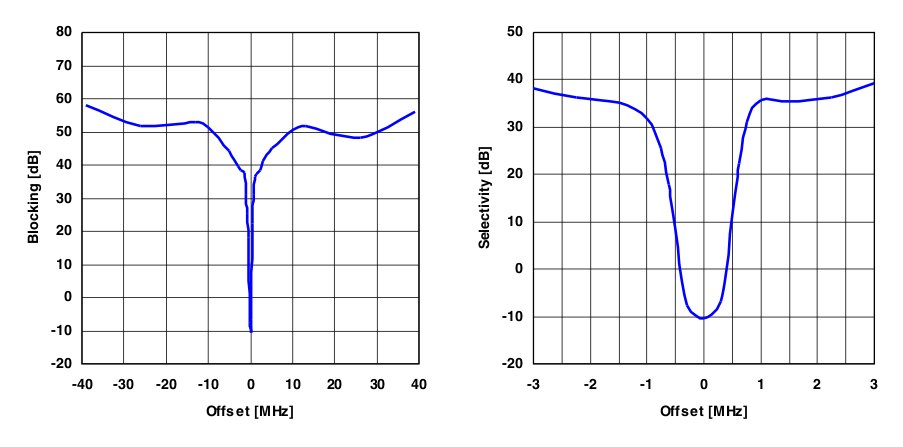
A.
Figure 5-23 Typical Selectivity at 250-kBaud Data Rate
NOTE:
868 MHz, 2-FSK, IF frequency is 304 kHz, digital channel filter bandwidth is 540 kHz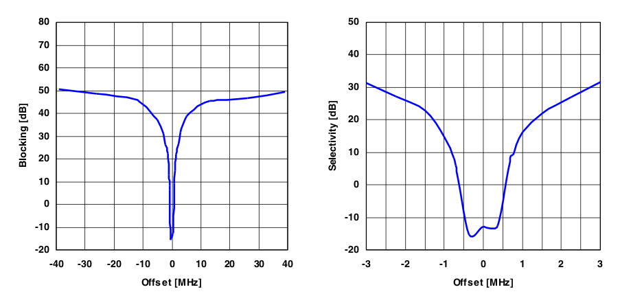
A.
Figure 5-24 Typical Selectivity at 500-kBaud Data Rate
NOTE:
868 MHz, 2-FSK, IF frequency is 355 kHz, digital channel filter bandwidth is 812 kHz5.40.13 Typical Sensitivity, 315 MHz, Sensitivity-Optimized Setting
| PARAMETER | DATA RATE (kBaud) | VCC | 2 V | 3 V | 3.6 V | UNIT | ||||||
|---|---|---|---|---|---|---|---|---|---|---|---|---|
| TA | –40°C | 25°C | 85°C | –40°C | 25°C | 85°C | –40°C | 25°C | 85°C | |||
| Sensitivity, 315MHz | 1.2 | –112 | –112 | –110 | –112 | –111 | –109 | –112 | –111 | –108 | dBm | |
| 38.4 | –105 | –105 | –104 | –105 | –103 | –102 | –105 | –104 | –102 | |||
| 250 | –95 | –95 | –92 | –94 | –95 | –92 | –95 | –94 | –91 | |||
5.40.14 Typical Sensitivity, 433 MHz, Sensitivity-Optimized Setting
| PARAMETER | DATA RATE (kBaud) | VCC | 2 V | 3 V | 3.6 V | UNIT | ||||||
|---|---|---|---|---|---|---|---|---|---|---|---|---|
| TA | –40°C | 25°C | 85°C | –40°C | 25°C | 85°C | –40°C | 25°C | 85°C | |||
| Sensitivity, 433MHz | 1.2 | –111 | –110 | –108 | –111 | –111 | –108 | –111 | –110 | –107 | dBm | |
| 38.4 | –104 | –104 | –101 | –104 | –104 | –101 | –104 | –103 | –101 | |||
| 250 | –93 | –94 | –91 | –93 | –93 | –90 | –93 | –93 | –90 | |||
5.40.15 Typical Sensitivity, 868 MHz, Sensitivity-Optimized Setting
| PARAMETER | DATA RATE (kBaud) | VCC | 2 V | 3 V | 3.6 V | UNIT | ||||||
|---|---|---|---|---|---|---|---|---|---|---|---|---|
| TA | –40°C | 25°C | 85°C | –40°C | 25°C | 85°C | –40°C | 25°C | 85°C | |||
| Sensitivity, 868MHz | 1.2 | –109 | –109 | –107 | –109 | –109 | –106 | –109 | –108 | –106 | dBm | |
| 38.4 | –102 | –102 | –100 | –102 | –102 | –99 | –102 | –101 | –99 | |||
| 250 | –90 | –90 | –88 | –89 | –90 | –87 | –89 | –90 | –87 | |||
| 500 | –84 | –84 | –81 | –84 | –84 | –80 | –84 | –84 | –80 | |||
5.40.16 Typical Sensitivity, 915 MHz, Sensitivity-Optimized Setting
| PARAMETER | DATA RATE (kBaud) | VCC | 2 V | 3 V | 3.6 V | UNIT | ||||||
|---|---|---|---|---|---|---|---|---|---|---|---|---|
| TA | –40°C | 25°C | 85°C | –40°C | 25°C | 85°C | –40°C | 25°C | 85°C | |||
| Sensitivity, 915MHz | 1.2 | –109 | –109 | –107 | –109 | –109 | –106 | –109 | –108 | –105 | dBm | |
| 38.4 | –102 | –102 | –100 | –102 | –102 | –99 | –103 | –102 | –99 | |||
| 250 | –92 | –92 | –89 | –92 | –92 | –88 | –92 | –92 | –88 | |||
| 500 | –87 | –86 | –81 | –86 | –86 | –81 | –86 | –85 | –80 | |||
5.40.17 RF Transmit
TA = 25°C, VCC = 3 V (unless otherwise noted)(1), PTX = +10 dBm (unless otherwise noted)| PARAMETER | FREQUENCY (MHz) | TEST CONDITIONS | MIN | TYP | MAX | UNIT | |
|---|---|---|---|---|---|---|---|
| Differential load impedance(1) | 315 | 122 + j31 | Ω | ||||
| 433 | 116 + j41 | ||||||
| 868/915 | 86.5 + j43 | ||||||
| Output power, highest setting(2) | 315 | Delivered to a 50-Ω single-ended load through the RF matching network of the CC430 reference design | +12 | dBm | |||
| 433 | +13 | ||||||
| 868 | +11 | ||||||
| 915 | +11 | ||||||
| Output power, lowest setting(2) | Delivered to a 50-Ω single-ended load through the RF matching network of the CC430 reference design | –30 | dBm | ||||
| Harmonics, radiated(3)(4)(5) |
433 | Second harmonic | –56 | dBm | |||
| Third harmonic | –57 | ||||||
| 868 | Second harmonic | –50 | |||||
| Third harmonic | –52 | ||||||
| 915 | Second harmonic | –50 | |||||
| Third harmonic | –54 | ||||||
| Harmonics, conducted | 315 | Frequencies below 960 MHz | +10 dBm CW | < –38 | dBm | ||
| Frequencies above 960 MHz | < –48 | ||||||
| 433 | Frequencies below 1 GHz | +10 dBm CW | –45 | ||||
| Frequencies above 1 GHz | < –48 | ||||||
| 868 | Second harmonic | +10 dBm CW | –59 | ||||
| Other harmonics | < –71 | ||||||
| 915 | Second harmonic | +11 dBm CW(6) | –53 | ||||
| Other harmonics | < –47 | ||||||
| Spurious emissions, conducted, harmonics not included(7) | 315 | Frequencies below 960 MHz | +10 dBm CW | < –58 | dBm | ||
| Frequencies above 960 MHz | < –53 | ||||||
| 433 | Frequencies below 1 GHz | +10 dBm CW | < –54 | ||||
| Frequencies above 1 GHz | < –54 | ||||||
| Frequencies within 47 to 74, 87.5 to 118, 174 to 230, 470 to 862 MHz | < –63 | ||||||
| 868 | Frequencies below 1 GHz | +10 dBm CW | < –46 | ||||
| Frequencies above 1 GHz | < –59 | ||||||
| Frequencies within 47 to 74, 87.5 to 118, 174 to 230, 470 to 862 MHz | < –56 | ||||||
| 915 | Frequencies below 960 MHz | +11 dBm CW | < –49 | ||||
| Frequencies above 960 MHz | < –63 | ||||||
| TX latency(8) | Serial operation | 8 | bits | ||||
(1) Differential impedance as seen from the RF port (RF_P and RF_N) toward the antenna. Follow the CC430 reference designs available from the TI website.
(2) Output power is programmable, and full range is available in all frequency bands. Output power may be restricted by regulatory limits. See also Application Note AN050 Using the CC1101 in the European 868MHz SRD Band (SWRA146) and design note DN013 Programming Output Power on CC1101 (SWRA168), which gives the output power and harmonics when using multi-layer inductors. The output power is then typically +10 dBm when operating at 868 or 915 MHz.
(3) The antennas used during the radiated measurements (SMAFF-433 from R.W.Badland and Nearson S331 868/915) play a part in attenuating the harmonics.
(4) Measured on EM430F6137RF900 with CW, maximum output power
(5) All harmonics are below –41.2 dBm when operating in the 902 through 928 MHz band.
(6) Requirement is –20 dBc under FCC 15.247
(7) All radiated spurious emissions are within the limits of ETSI. Also see design note DN017 CC11xx 868 or 915 MHz RF Matching (SWRA168).
(8) Time from sampling the data on the transmitter data input pin until it is observed on the RF output ports
5.40.18 Optimum PATABLE Settings for Various Output Power Levels and Frequency Bands
TA = 25°C, VCC = 3 V (unless otherwise noted)(1)| OUTPUT POWER (dBm) | PATABLE SETTING | |||
|---|---|---|---|---|
| 315 MHz | 433 MHz | 868 MHz | 915 MHz | |
| –30 | 0x12 | 0x05 | 0x03 | 0x03 |
| –12 | 0x33 | 0x26 | 0x25 | 0x25 |
| –6 | 0x29 | 0x2D | 0x2D | 0x2D |
| 0 | 0x51 | 0x50 | 0x8D | 0x8D |
| 10 | 0xC4 | 0xC4 | 0xC3 | 0xC3 |
| Maximum | 0xC0 | 0xC0 | 0xC0 | 0xC0 |
5.40.19 Typical Output Power, 315 MHz(1)
| PARAMETER | PATABLE SETTING | VCC | 2 V | 3 V | 3.6 V | UNIT | ||||||
|---|---|---|---|---|---|---|---|---|---|---|---|---|
| TA | –40°C | 25°C | 85°C | –40°C | 25°C | 85°C | –40°C | 25°C | 85°C | |||
| Output power, 315 MHz | 0xC0 (max) | 11.9 | 11.8 | 11.8 | dBm | |||||||
| 0xC4 (10 dBm) | 10.3 | 10.3 | 10.3 | |||||||||
| 0xC6 (default) | 9.3 | |||||||||||
| 0x51 (0 dBm) | 0.7 | 0.6 | 0.7 | |||||||||
| 0x29 (–6 dBm) | –6.8 | –5.6 | –5.3 | |||||||||
5.40.20 Typical Output Power, 433 MHz(1)
| PARAMETER | PATABLE SETTING | VCC | 2 V | 3 V | 3.6 V | UNIT | ||||||
|---|---|---|---|---|---|---|---|---|---|---|---|---|
| TA | –40°C | 25°C | 85°C | –40°C | 25°C | 85°C | –40°C | 25°C | 85°C | |||
| Output power, 433 MHz | 0xC0 (max) | 12.6 | 12.6 | 12.6 | dBm | |||||||
| 0xC4 (10 dBm) | 10.3 | 10.2 | 10.2 | |||||||||
| 0xC6 (default) | 10.0 | |||||||||||
| 0x50 (0 dBm) | 0.3 | 0.3 | 0.3 | |||||||||
| 0x2D (–6 dBm) | –6.4 | –5.4 | –5.1 | |||||||||
5.40.21 Typical Output Power, 868 MHz(1)
| PARAMETER | PATABLE SETTING | VCC | 2 V | 3 V | 3.6 V | UNIT | ||||||
|---|---|---|---|---|---|---|---|---|---|---|---|---|
| TA | –40°C | 25°C | 85°C | –40°C | 25°C | 85°C | –40°C | 25°C | 85°C | |||
| Output power, 868 MHz | 0xC0 (max) | 11.9 | 11.2 | 10.5 | 11.9 | 11.2 | 10.5 | 11.9 | 11.2 | 10.5 | dBm | |
| 0xC3 (10 dBm) | 10.8 | 10.1 | 9.4 | 10.8 | 10.1 | 9.4 | 10.7 | 10.1 | 9.4 | |||
| 0xC6 (default) | 8.8 | |||||||||||
| 0x8D (0 dBm) | 1.0 | 0.3 | –0.3 | 1.1 | 0.3 | –0.3 | 1.1 | 0.3 | –0.3 | |||
| 0x2D (–6 dBm) | –6.5 | –6.8 | –7.3 | –5.3 | –5.8 | –6.3 | –4.9 | –5.4 | –6.0 | |||
5.40.22 Typical Output Power, 915 MHz(1)
| PARAMETER | PATABLE SETTING | VCC | 2 V | 3 V | 3.6 V | UNIT | ||||||
|---|---|---|---|---|---|---|---|---|---|---|---|---|
| TA | –40°C | 25°C | 85°C | –40°C | 25°C | 85°C | –40°C | 25°C | 85°C | |||
| Output power, 915 MHz | 0xC0 (max) | 12.2 | 11.4 | 10.6 | 12.1 | 11.4 | 10.7 | 12.1 | 11.4 | 10.7 | dBm | |
| 0xC3 (10 dBm) | 11.0 | 10.3 | 9.5 | 11.0 | 10.3 | 9.5 | 11.0 | 10.3 | 9.6 | |||
| 0xC6 (default) | 8.8 | |||||||||||
| 0x8D (0 dBm) | 1.9 | 1.0 | 0.3 | 1.9 | 1.0 | 0.3 | 1.9 | 1.1 | 0.3 | |||
| 0x2D (–6 dBm) | –5.5 | –6.0 | –6.5 | –4.3 | –4.8 | –5.5 | –3.9 | –4.4 | –5.1 | |||
5.40.23 Frequency Synthesizer Characteristics
TA = 25°C, VCC = 3 V (unless otherwise noted)(1)MIN figures are given using a 27MHz crystal. TYP and MAX figures are given using a 26MHz crystal.
| PARAMETER | TEST CONDITIONS | MIN | TYP | MAX | UNIT |
|---|---|---|---|---|---|
| Programmed frequency resolution(1) | 26- to 27-MHz crystal | 397 | fXOSC/216 | 412 | Hz |
| Synthesizer frequency tolerance(2) | ±40 | ppm | |||
| RF carrier phase noise | 50-kHz offset from carrier | –95 | dBc/Hz | ||
| 100-kHz offset from carrier | –94 | ||||
| 200-kHz offset from carrier | –94 | ||||
| 500-kHz offset from carrier | –98 | ||||
| 1-MHz offset from carrier | –107 | ||||
| 2-MHz offset from carrier | –112 | ||||
| 5-MHz offset from carrier | –118 | ||||
| 10-MHz offset from carrier | –129 | ||||
| PLL turnon or hop time(3) | Crystal oscillator running | 85.1 | 88.4 | 88.4 | µs |
| PLL RX-to-TX settling time(4) | 9.3 | 9.6 | 9.6 | µs | |
| PLL TX-to-RX settling time(5) | 20.7 | 21.5 | 21.5 | µs | |
| PLL calibration time(6) | 694 | 721 | 721 | µs |
(1) The resolution (in Hz) is equal for all frequency bands.
(2) Depends on crystal used. Required accuracy (including temperature and aging) depends on frequency band and channel bandwidth and spacing.
(3) Time from leaving the IDLE state until arriving in the RX, FSTXON, or TX state, when not performing calibration.
(4) Settling time for the 1-IF frequency step from RX to TX
(5) Settling time for the 1-IF frequency step from TX to RX
(6) Calibration can be initiated manually or automatically before entering or after leaving RX/TX.
5.40.24 Typical RSSI_offset Values
TA = 25°C, VCC = 3 V (unless otherwise noted)(1)| DATA RATE (kBaud) | RSSI_OFFSET (dB) | |
|---|---|---|
| 433 MHz | 868 MHz | |
| 1.2 | 74 | 74 |
| 38.4 | 74 | 74 |
| 250 | 74 | 74 |
| 500 | 74 | 74 |
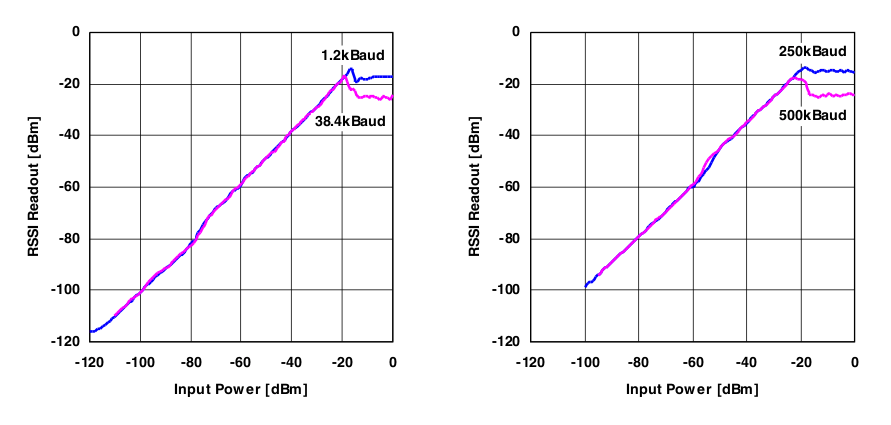 Figure 5-25 Typical RSSI Value vs Input Power Level for Different Data Rates at 868 MHz
5.41 3D LF Front-End Parameters
5.41.1 Recommended Operating Conditions
| MIN | NOM | MAX | UNIT | ||
|---|---|---|---|---|---|
| VBAT | Supply voltage range during LF operation | 2.0 | 3.6 | V | |
| RF crystal load capacitance | 10 | 13 | 20 | pF | |
| RF crystal effective series resistance | 100 | Ω | |||
5.41.2 Resonant Circuits – LF Front End
The resonance circuit quality factor QOP can have a wide range between 10 and 120. The resonance frequency can be trimmed by the embedded trimming capacitor array.5.41.3 External Antenna Coil – LF Front End
The antenna coil LR, resonant capacitor CR and charge capacitor CL are external components with following recommended parameters| PARAMETER | TEST CONDITIONS | MIN | TYP | MAX | UNIT | |
|---|---|---|---|---|---|---|
| LR1 | Equivalent inductance | 25°C, f = 134.2 kHz | 7.37 | 7.6 | 7.81 | mH |
| LR2 | Equivalent inductance | 25°C, f = 134.2 kHz | 4.37 | 4.5 | 4.63 | mH |
| dLR/LRdT | Temperature coefficient of LR | –40°C to 85°C | 250 | ppm/°C | ||
| QLRT | Quality factor of LR | –40°C to 85°C | 10 | 150 | ||
5.41.4 Resonant Circuit Capacitor – LF Front End
The input capacitance of the RF pins CRF is the sum of parasitic capacitances of circuit blocks connected to the RF pin. The trimming capacitors are internal capacitances and can be programmed on or off. The resonance capacitor CR is an external component and is not part of this IC.5.41.5 Charge Capacitor – LF Front End
| PARAMETER | TEST CONDITIONS | MIN | TYP | MAX | UNIT | |
|---|---|---|---|---|---|---|
| CL | Charge capacitor (dCL = ±10%) | 25°C, QOP = 134.2 kHz | 198 | 220 | 242 | nF |
| dCL(T) | Temperature coefficient of CL | –40°C to 85°C | –10% | 10% | ||
| Dielectric of CL | XR7 | |||||
| DCL(t) | Charge capacitor aging | 100000 h | –10% | 0% | ||
5.41.6 LF Wake Receiver Electrical Characteristics
over operating free-air temperature range (unless otherwise noted)| PARAMETER | TEST CONDITIONS | MIN | TYP | MAX | UNIT | |
|---|---|---|---|---|---|---|
| fRES,PE | Resonant circuit frequency | 25°C | 110 | 140 | kHz | |
| tWakeUp | Wake-up time | 500 | 560 | 1000 | µs | |
| IPESBWP | Standby current | Wake pattern A active, wake pattern B off, regular sensitivity, VBAT = 3 V |
4.4 | µA | ||
| VWAKEA | Sensitivity A (regular) | Configured to highest sensitivity | 2.6 | 3.7 | 6.2 | mVpp |
| VWAKEA | Sensitivity A (regular) | Configured to lowest sensitivity | 9 | 13.5 | 23 | mVpp |
| VWAKEA | Sensitivity A (high sensitivity mode) | Configured to highest sensitivity and high sensitivity mode | 0.3 | 0.5 | 0.9 | mVpp |
| VWAKEB | Sensitivity B | Configured to highest sensitivity | 2.3 | 4.2 | 7.5 | mVpp |
| VWAKEB | Sensitivity B | Configured to lowest sensitivity | 50 | 110 | 200 | mVpp |
| VRF | Maximum RF input voltage | 10 | Vpp | |||
| S/N | Wake pattern detection error rate (S/N) | 10 | dB | |||
| tsA | WDE settling time (wake A, low sensitivity) | 500 | µs | |||
| tsAh | WDE settling time (wake A, high sensitivity) | 600 | µs | |||
| ts\B | WDE settling time (wake B) | 2000 | µs | |||
| tresA | WDE resettling time (strong burst recovery time) | Step VRF 2Vpp to 10mVpp | 3000 | µs | ||
5.41.7 RSSI - LF Wake Receiver Electrical Characteristics
over operating free-air temperature range (unless otherwise noted)| PARAMETER | MIN | TYP | MAX | UNIT | |
|---|---|---|---|---|---|
| DR | Dynamic range | 72 | dB | ||
| VRF | Input voltage range | 0.002 | 8 | Vpp | |
| A | RSSI linear coefficient | 28 | |||
| B | RSSI constant coefficient | 180 | |||
| #RSSI | Number of RSSI values | 128 | |||
| Verr16mV | Absolute RSSI error at VRF = 16 mVpp | –1.28 | 1.28 | mVpp | |
| err16mV | Relative RSSI error VRF ≥ 16 mVpp | –8% | 8% | ||
| Verr2mV | Absolute RSSI error at VRF = 2 mVpp | –0.4 | 0.4 | mVpp | |
| err2mV | Relative RSSI error at VRF = 2 mVpp | –20% | 20% | ||
| Vmin | Resolution at VRF = 2 mVpp | 0.14 | mV | ||
| t | Measurement time (all three channels) | 2 | ms | ||