SLLSEE8B September 2013 – September 2014 SN65LVDS822
PRODUCTION DATA.
- 1 Features
- 2 Applications
- 3 Description
- 4 Revision History
- 5 Description (Continued)
- 6 Pin Configuration and Functions
- 7 Specifications
- 8 Parameter Measurement Information
- 9 Detailed Description
- 10Application and Implementation
- 11Power Supply Recommendations
- 12Layout
- 13Device and Documentation Support
- 14Mechanical, Packaging, and Orderable Information
Package Options
Mechanical Data (Package|Pins)
- RGZ|48
Thermal pad, mechanical data (Package|Pins)
- RGZ|48
Orderable Information
1 Features
- 4:27 LVDS-to-CMOS Deserializer
- Pixel Clock Range of 4 MHz to 54 MHz, for Resolutions of 160 × 120 to 1024 × 600
- Special 2:27 Mode With 14x Sampling Allows Using Just Two Data Lanes
- Very Low EMI With 3-Way Selectable CMOS Slew Rate
- Supports Single 3.3-V Power Supply; VDDIO Allows 1.8 V to 3.3 V for Flexible Panel Support
- Clock Output is Rising or Falling Edge
- Bus-Swap Feature for Flexible PCB Layout
- Integrated Switchable Input Termination
- All Input Pins are Failsafe; ±3 kV HBM ESD Protection
- 7-mm x 7-mm 48-Pin VQFN With 0.5-mm Pitch
- Compatible With TIA/EIA-644-A Transmitters
2 Applications
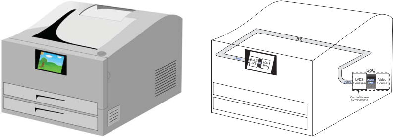
- Printers
- Appliances With an LCD
- Digital Cameras
3 Description
The SN65LVDS822 is an advanced FlatLink™ low-voltage differential signal (LVDS) receiver designed on a modern CMOS process. The device has several unique features, including three selectable CMOS output slew rates, CMOS output voltage support of 1.8 V to 3.3 V, a pinout swap option, integrated differential termination (configurable), an automatic low-power mode, and deserialization modes of 4:27 and 2:27. The device is compatible with TI FlatLink™ transmitters such as the SN75LVDS83B, SN65LVDS93A, and standard industry LVDS transmitters that comply with TIA/EIA 644-A.
The SN65LVDS822 features an automatic low-power Standby Mode, activated when the LVDS clock is disabled. The device enters an even lower-power Shutdown Mode with a low voltage applied to pin SHTDN#.
The SN65LVDS822 is packaged in a 48-pin 7-mm x 7-mm Plastic Quad Flatpack No-Lead (QFN) with a 0.5-mm pin pitch, and operates through an industrial ambient temperature range of –40°C to 85°C.
Device Information(1)
| PART NUMBER | PACKAGE | BODY SIZE (NOM) |
|---|---|---|
| SN65LVDS822 | VQFN (48) | 7.00 mm x 7.00 mm |
- For all available packages, see the orderable addendum at the end of the datasheet.