SCES220U April 1999 – April 2017 SN74LVC1G79
PRODUCTION DATA.
- 1 Features
- 2 Applications
- 3 Description
- 4 Revision History
- 5 Pin Configuration and Functions
-
6 Specifications
- 6.1 Absolute Maximum Ratings
- 6.2 ESD Ratings
- 6.3 Recommended Operating Conditions
- 6.4 Thermal Information
- 6.5 Electrical Characteristics
- 6.6 Timing Requirements: TA = -40°C to +85°C
- 6.7 Timing Requirements: TA = -40°C to +125°C
- 6.8 Switching Characteristics: CL = 15 pF, TA = -40°C to +85°C
- 6.9 Switching Characteristics: CL = 30 or 50 pF, TA = -40°C to +85°C
- 6.10 Switching Characteristics: CL = 30 pF or 50 pF, TA = -40°C to +125°C
- 6.11 Operating Characteristics
- 6.12 Typical Characteristics
- 7 Parameter Measurement Information
- 8 Detailed Description
- 9 Application and Implementation
- 10Power Supply Recommendations
- 11Layout
- 12Device and Documentation Support
- 13Mechanical, Packaging, and Orderable Information
Package Options
Refer to the PDF data sheet for device specific package drawings
Mechanical Data (Package|Pins)
- DBV|5
- DCK|5
- DRL|5
- YZP|5
Thermal pad, mechanical data (Package|Pins)
Orderable Information
1 Features
- Available in the Texas Instruments
NanoFree™ Package - Latch-Up Performance Exceeds 100 mA Per JESD 78, Class II
- ESD Protection Exceeds JESD 22
- 2000-V Human-Body Model (A114-A)
- 200-V Machine Model (A115-A)
- 1000-V Charged-Device Model (C101)
- Supports 5-V VCC Operation
- Inputs Accept Voltages to 5.5 V
- Supports Down Translation to VCC
- Max tpd of 6 ns at 3.3 V and 50 pF load
- Low Power Consumption, 10-µA Max ICC
- ±24-mA Output Drive at 3.3 V
- Ioff supports Partial-Power-Down Mode and Back-Drive Protection
2 Applications
- Test and Measurement
- Enterprise Switching
- Telecom Infrastructure
- Personal Electronics
- White Goods
3 Description
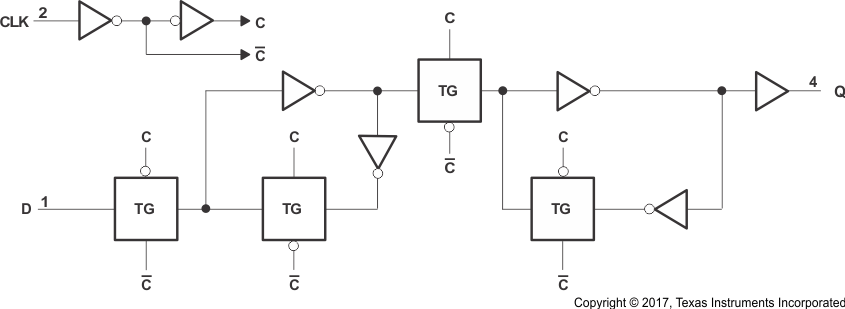
The SN74LVC1G79 device is a single positive-edge-triggered D-type flip-flop that is designed for 1.65-V to 5.5-V VCC operation.
When data at the data (D) input meets the setup time requirement, the data is transferred to the Q output on the positive-going edge of the clock pulse. Clock triggering occurs at a voltage level and is not directly related to the rise time of the clock pulse. Following the hold-time interval, data at the D input can be changed without affecting the level at the output.
NanoFree™ package technology is a major breakthrough in IC packaging concepts, using the die as the package.
This device is fully specified for partial-power-down applications using Ioff. The Ioff circuitry disables the outputs when the device is powered down. This inhibits current backflow into the device which prevents damage to the device.
Device Information(1)
| PART NUMBER | PACKAGE | BODY SIZE |
|---|---|---|
| SN74LVC1G79DBV | SOT-23 (5) | 2.90 mm × 1.60 mm |
| SN74LVC1G79DCK | SC70 (5) | 2.00 mm × 1.25 mm |
| SN74LVC1G79DRL | SOT (5) | 1.60 mm × 1.20 mm |
| SN74LVC1G79YZP | DSBGA (5) | 1.14 mm × 0.91 mm |
- For all available packages, see the orderable addendum at the end of the data sheet.
Logic Diagram (Positive Logic)
