SLRS007C November 1986 – January 2015 SN754410
PRODUCTION DATA.
- 1 Features
- 2 Applications
- 3 Description
- 4 Simplified Schematic
- 5 Revision History
- 6 Pin Configuration and Functions
- 7 Specifications
- 8 Parameter Measurement Information
- 9 Detailed Description
- 10Application and Implementation
- 11Power Supply Recommendations
- 12Layout
- 13Device and Documentation Support
- 14Mechanical, Packaging, and Orderable Information
Package Options
Refer to the PDF data sheet for device specific package drawings
Mechanical Data (Package|Pins)
- NE|16
Thermal pad, mechanical data (Package|Pins)
Orderable Information
8 Parameter Measurement Information
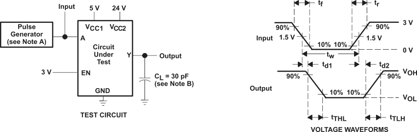
A. The pulse generator has the following characteristics: tr ≤10 ns, tf ≤10 ns, tw = 10 µs, PRR = 5 kHz, ZO = 50 Ω
B. CL includes probe and jig capacitance.
Figure 3. Test Circuit and Switching Times from Data Inputs
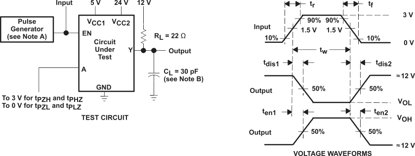
A. The pulse generator has the following characteristics: tr ≤10 ns, tf ≤10 ns, tw = 10 µs, PRR = 5 kHz, ZO = 50 Ω
B. CL includes probe and jig capacitance.
Figure 4. Test Circuit and Switching Times from Enable Inputs