SLOS795F September 2013 – October 2017 TAS5414C-Q1 , TAS5424C-Q1
PRODUCTION DATA.
- 1 Features
- 2 Applications
- 3 Description
- 4 Revision History
- 5 Pin Configuration and Functions
- 6 Specifications
- 7 Detailed Description
- 8 Application and Implementation
- 9 Power Supply Recommendations
- 10Layout
- 11Device and Documentation Support
- 12Mechanical, Packaging, and Orderable Information
Package Options
Refer to the PDF data sheet for device specific package drawings
Mechanical Data (Package|Pins)
- PHD|64
Thermal pad, mechanical data (Package|Pins)
- PHD|64
Orderable Information
1 Features
- AEC-Q100 Qualified for Automotive Applications
- Device Temperature: –55°C to 125°C Ambient
- Device HBM Classification Level: ±2500 V
- Device CDM Classification Level: ±500 V
- TAS5414C-Q1 – Single-Ended Input
- TAS5424C-Q1 – Differential Input
- Four-Channel Digital Power Amplifier
- Four Analog Inputs, Four BTL Power Outputs
- Typical Output Power at 10% THD+N
- 28 W/Ch Into 4 Ω at 14.4 V
- 50 W/Ch Into 2 Ω at 14.4 V
- 79 W/Ch Into 4 Ω at 24 V
- 150 W/Ch Into 2 Ω at 24 V (PBTL)
- Channels Can Be Paralleled (PBTL) for High-Current Applications
- THD+N < 0.02%, 1 kHz, 1 W Into 4 Ω
- Patented Pop- and Click-Reduction Technology
- Soft Muting With Gain Ramp Control
- Common-Mode Ramping
- Patented AM Interference Avoidance
- Patented Cycle-by-Cycle Current Limit
- 75-dB PSRR
- Four-Address I2C Serial Interface for Device Configuration and Control
- Channel Gains: 12-dB, 20-dB, 26-dB, 32-dB
- Load Diagnostic Functions:
- Output Open and Shorted Load
- Output-to-Power and -to-Ground Shorts
- Patented Tweeter Detection
- Protection and Monitoring Functions:
- Short-Circuit Protection
- Load-Dump Protection to 50 V
- Fortuitous Open-Ground and -Power Tolerant
- Patented Output DC Level Detection While Music Playing
- Overtemperature Protection
- Over- and Undervoltage Conditions
- Clip Detection
- 44-Pin PSOP3 (DKE) Power SOP Package With Heat Slug Up for TAS5424C-Q1
- 64-Pin QFP (PHD) Power Package With Heat Slug Up for TAS5414C-Q1
- Designed for Automotive EMC Requirements
- ISO9000:2002 TS16949 Certified
- –40°C to 105°C Ambient Temperature Range
2 Applications
OEM/Retail Head Units and Amplifier Modules Where Feature Densities and System Configurations Require Reduction in Heat From the Audio Power Amplifier
3 Description
The TAS5414C-Q1 and TAS5424C-Q1 are four-channel digital audio amplifiers designed for use in automotive head units and external amplifier modules. They provide four channels at 23 W continuously into 4 Ω at less than 1% THD+N from a 14.4-V supply. Each channel can also deliver 38 W into 2 Ω at 1% THD+N. The TAS5414C-Q1 uses single-ended analog inputs, whereas the TAS5424C-Q1 employs differential inputs for increased immunity to common-mode system noise. The digital PWM topology of the device provides dramatic improvements in efficiency over traditional linear amplifier solutions. This reduces the power dissipated by the amplifier by a factor of ten under typical music playback conditions. The device incorporates all the functionality needed to perform in the demanding OEM applications area. The devices have built-in load diagnostic functions for detecting and diagnosing misconnected outputs to help to reduce test time during the manufacturing process.
Device Information(1)
| PART NUMBER | PACKAGE | BODY SIZE (NOM) |
|---|---|---|
| TAS5414C-Q1 | HTQFP (64) | 14.00mm x 14.00mm |
| TAS5424C-Q1 | HSSOP (44) | 3.50mm x 15.90mm |
- For all available packages, see the orderable addendum at the end of the datasheet.
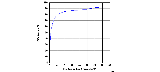
Power vs Efficiency
