SLOS955 December 2016 TAS5414C
PRODUCTION DATA.
- 1 Features
- 2 Applications
- 3 Description
- 4 Revision History
- 5 Pin Configuration and Functions
- 6 Specifications
-
7 Detailed Description
- 7.1 Overview
- 7.2 Functional Block Diagram
- 7.3 Feature Descption
- 7.4 Device Functional Modes
- 7.5 Programming
- 7.6
Register Maps
- 7.6.1 Register Summary
- 7.6.2 Registers
- 7.6.3 Fault Register 2 (0x01) Protection
- 7.6.4 Diagnostic Register 1 (0x02) Load Diagnostics
- 7.6.5 Diagnostic Register 2 (0x03) Load Diagnostics
- 7.6.6 External Status Register 1 (0x04) Fault Detection
- 7.6.7 External Status Register 2 (0x05) Output State of Individual Channels
- 7.6.8 External Status Register 3 (0x06) Play and Mute Modes
- 7.6.9 External Status Register 4 (0x07) Load Diagnostics
- 7.6.10 External Control Register 1 (0x08) Gain Select
- 7.6.11 External Control Register 2 (0x09) Overcurrent Control
- 7.6.12 External Control Register 3 (0x0A) Switching Frequency Select and Clip_OTW Configuration
- 7.6.13 External Control Register 4 (0x0B) Load Diagnostics and Master/Slave Control
- 7.6.14 External Control Register 5 (0x0C) Output Control
- 7.6.15 External Control Register 6 (0x0D) Output Control
- 7.6.16 External Control Register 7 (0x10) Miscellaneous Selection
- 7.6.17 External Status Register 5 (0x13) Overtemperature and Thermal Foldback Status
- 8 Application and Implementation
- 9 Power Supply Recommendations
- 10Layout
- 11Device and Documentation Support
- 12Mechanical, Packaging, and Orderable Information
Package Options
Mechanical Data (Package|Pins)
- PHD|64
Thermal pad, mechanical data (Package|Pins)
- PHD|64
Orderable Information
10 Layout
10.1 Layout Guidelines
- The EVM layout optimizes for low noise and EMC performance.
- The TAS5414C device has a thermal pad up, therefore a the layout must take into account an external heatsink.
- Layout also affects EMC performance.
- The EVM PCB illustrations form the basis for the layout discussions.
10.2 Layout Example
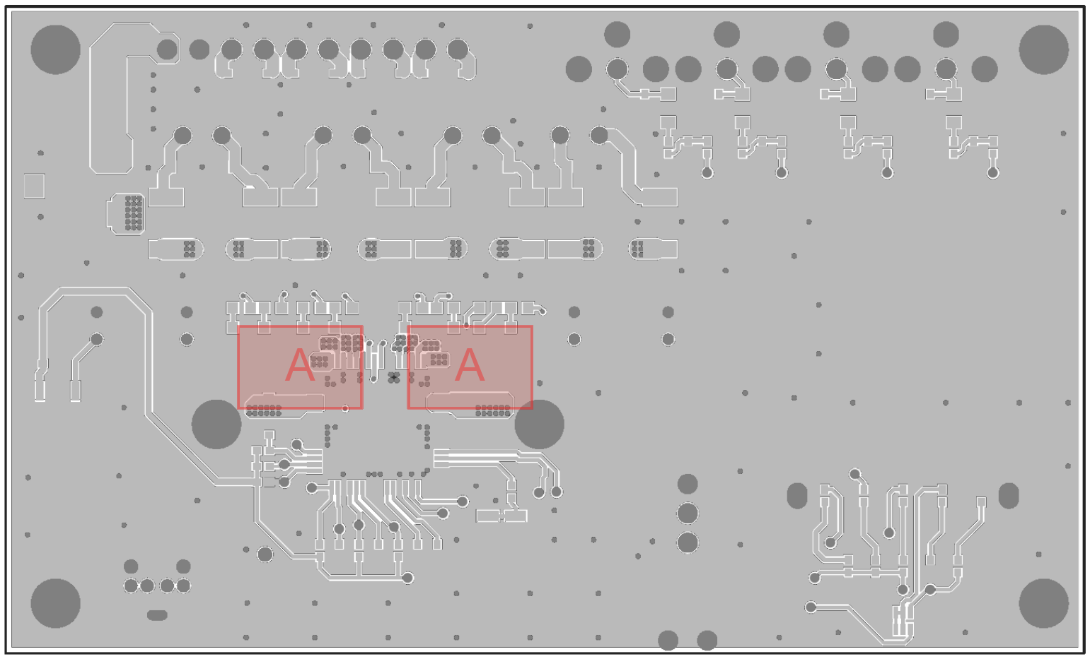
The areas indicated by the label "A", are critical to proper operation and EMC layout. The PVDD and ground decoupling capacitors should be close to the device. These decoupling capacitors must be on both groups of PVDD pins to ground. The ground connections of the snubber circuits must also be close to the grounds of the device. The grounds of the decoupling caps and the snubber circuits do not pass through vias before connecting to the device ground. This reduces the ground impedance for EMC mititgation.
 Figure 39. Top Layer
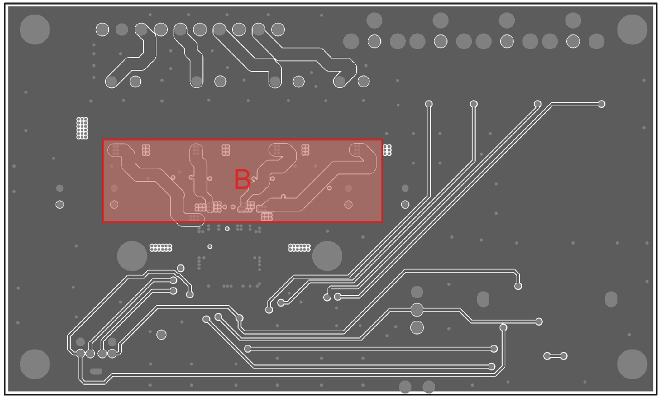
The area referenced as "B" are nets in the PCB layout that have large high frequency switching signals. These should be buried on an inner layer with ground planes on layers above and below to mitigate EMC.
 Figure 40. A Mid Layer
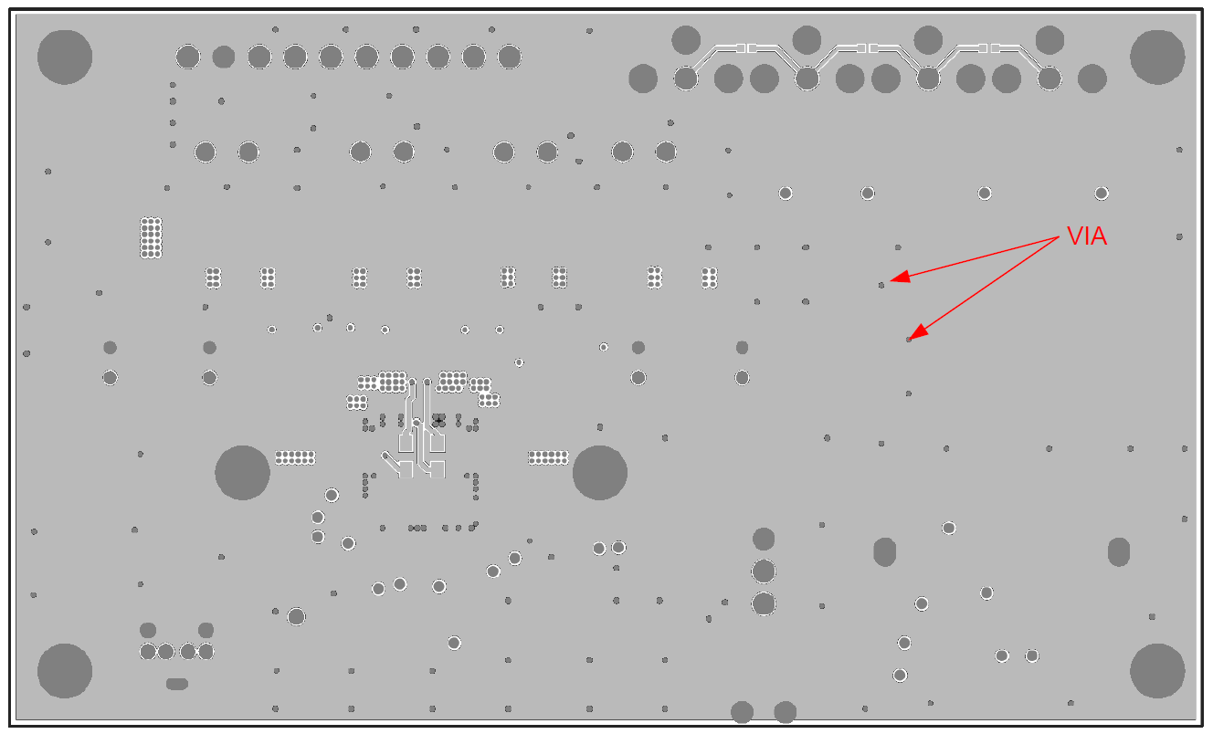
The bottom layer in the EVM is almost all ground plane. It can be seen that the other layers have ground planes that fill unused areas. All these ground planes need to be connected together through many vias to reduce the impedance between the ground layers. This allows for reduced EMI.
 Figure 41. Bottom Layer
10.3 Thermal Consideration
The design of the thermally augmented package is for interface directly to heat sinks using a thermal interface compound (for example, Arctic Silver, Ceramique thermal compound). The heat sink then absorbs heat from the ICs and couples it to the local air. With proper thermal management this process can reach equilibrium at a lower temperature and heat can be continually removed from the ICs. Because of the device efficiency, heat sinks can be smaller than those required for linear amplifiers of equivalent performance.
RθJA is a system thermal resistance from junction to ambient air. As such, it is a system parameter with the following components:
- RθJC (the thermal resistance from junction to case, or in this case the heat slug)
- Thermal resistance of the thermal grease
- Thermal resistance of the heat sink
One can calculate the thermal resistance of the thermal grease from the exposed heat slug area and the manufacturer's value for the area thermal resistance of the thermal grease (expressed in °C-in2/W or °C-mm2/W). The area thermal resistance of the example thermal grease with a 0.001-inch (0.0254-mm) thick layer is about 0.007°C-in2/W (4.52°C-mm2/W). The approximate exposed heat slug size is as follows:
| 64-pin QFP | 0.099 in2 (64 mm2) |
Dividing the example area thermal resistance of the thermal grease by the area of the heat slug gives the actual resistance through the thermal grease:
| 64-pin QFP | 0.07°C/W |
The thermal resistance of thermal pads is generally considerably higher than a thin thermal-grease layer. Thermal tape has an even higher thermal resistance and should not be used at all. The heat-sink vendor generally predicts heat sink thermal resistance, either modeled using a continuous-flow dynamics (CFD) model, or measured.
Thus, for a single monaural channel in the IC, the system RθJA = RθJC + thermal-grease resistance + heat-sink resistance.
Table 25 indicates modeled parameters for one device on a heat sink. The junction temperature setting is at 115°C while delivering 20 watts per channel into 4-Ω loads with no clipping. The assumed thickness of the thermal grease is about 0.001 inches (0.0254 mm).
Table 25. QFP Package Modeled Parameters
| DEVICE | 64-PIN QFP |
|---|---|
| Ambient temperature | 25°C |
| Power to load | 20 W × 4 |
| Power dissipation | 1.9 W × 4 |
| ΔT inside package | 7.6°C |
| ΔT through thermal grease | 0.46°C |
| Required heatsink thermal resistance | 10.78°C/W |
| Junction temperature | 115°C |
| System RθJA | 11.85°C/W |
| RθJA × power dissipation | 90°C |
10.4 Electrical Connection of Heat Slug and Heat Sink
Electrically connect the heat sink attached to the heat slug of the device to GND, or leave it floating. Do not connect the heat slug to any other electrical node.
10.5 EMI Considerations
EMI performance depends on both careful integrated circuit design and good system-level design. Controlling sources of electromagnetic interference (EMI) was a major consideration in all aspects of the design.
The design has minimal parasitic inductances due to the short leads on the package. This dramatically reduces the EMI that results from current passing from the die to the system PCB. Each channel also operates at a different phase. The phase between channels is I2C selectable to either 45° or 180°, to reduce EMI caused by high-current switching. The design also incorporates circuitry that optimizes output transitions that cause EMI.