SNAS670 July   2015 TDC1011-Q1

PRODUCTION DATA.  

  1. Features
  2. Applications
  3. Description
  4. Revision History
  5. Pin Configuration and Functions
  6. Specifications
    1. 6.1 Absolute Maximum Ratings
    2. 6.2 ESD Ratings
    3. 6.3 Recommended Operating Conditions
    4. 6.4 Thermal Information
    5. 6.5 Electrical Characteristics
    6. 6.6 Timing Requirements
    7. 6.7 Switching Characteristics
    8. 6.8 Typical Characteristics
  7. Parameter Measurement Information
  8. Detailed Description
    1. 8.1 Overview
    2. 8.2 Functional Block Diagram
    3. 8.3 Feature Description
      1. 8.3.1 Transmitter Signal Path
      2. 8.3.2 Receiver Signal Path
      3. 8.3.3 Low Noise Amplifier (LNA)
      4. 8.3.4 Programmable Gain Amplifier (PGA)
      5. 8.3.5 Receiver Filters
      6. 8.3.6 Comparators for STOP Pulse Generation
        1. 8.3.6.1 Threshold Detector and DAC
        2. 8.3.6.2 Zero-cross Detect Comparator
        3. 8.3.6.3 Event Manager
      7. 8.3.7 Common-mode Buffer (VCOM)
      8. 8.3.8 Temperature Sensor
        1. 8.3.8.1 Temperature Measurement with Multiple RTDs
        2. 8.3.8.2 Temperature Measurement with a Single RTD
    4. 8.4 Device Function Description
      1. 8.4.1 Time-of-Flight Measurement Mode
        1. 8.4.1.1 Liquid Level or Fluid Identification
      2. 8.4.2 State Machine
      3. 8.4.3 TRANSMIT Operation
        1. 8.4.3.1 Transmission Pulse Count
        2. 8.4.3.2 TX 180° Pulse Shift
        3. 8.4.3.3 Transmitter Damping
      4. 8.4.4 RECEIVE Operation
        1. 8.4.4.1 Single Echo Receive Mode
        2. 8.4.4.2 Multiple Echo Receive Mode
      5. 8.4.5 Timing
        1. 8.4.5.1 Timing Control and Frequency Scaling (CLKIN)
        2. 8.4.5.2 TX/RX Measurement Sequencing and Timing
      6. 8.4.6 Time-of-Flight (TOF) Control
        1. 8.4.6.1 Short TOF Measurement
        2. 8.4.6.2 Standard TOF Measurement
        3. 8.4.6.3 Standard TOF Measurement with Power Blanking
        4. 8.4.6.4 Common-mode Reference Settling Time
        5. 8.4.6.5 TOF Measurement Interval
      7. 8.4.7 Error Reporting
    5. 8.5 Programming
      1. 8.5.1 Serial Peripheral Interface (SPI)
        1. 8.5.1.1 Chip Select Bar (CSB)
        2. 8.5.1.2 Serial Clock (SCLK)
        3. 8.5.1.3 Serial Data Input (SDI)
        4. 8.5.1.4 Serial Data Output (SDO)
    6. 8.6 Register Maps
      1. 8.6.1 TDC1011 Registers
        1. 8.6.1.1  CONFIG_0 Register (address = 0h) [reset = 45h]
        2. 8.6.1.2  CONFIG_1 Register (address = 1h) [reset = 40h]
        3. 8.6.1.3  CONFIG_2 Register (address = 2h) [reset = 0h]
        4. 8.6.1.4  CONFIG_3 Register (address 3h) [reset = 3h]
        5. 8.6.1.5  CONFIG_4 Register (address = 4h) [reset = 1Fh]
        6. 8.6.1.6  TOF_1 Register (address = 5h) [reset = 0h]
        7. 8.6.1.7  TOF_0 Register (address = 6h) [reset = 0h]
        8. 8.6.1.8  ERROR_FLAGS Register (address = 7h) [reset = 0h]
        9. 8.6.1.9  TIMEOUT Register (address = 8h) [reset = 19h]
        10. 8.6.1.10 CLOCK_RATE Register (address = 9h) [reset = 0h]
  9. Application and Implementation
    1. 9.1 Application Information
    2. 9.2 Typical Applications
      1. 9.2.1 Level and Fluid Identification Measurements
        1. 9.2.1.1 Design Requirements
        2. 9.2.1.2 Detailed Design Procedure
          1. 9.2.1.2.1 Level Measurements
          2. 9.2.1.2.2 Fluid Identification
        3. 9.2.1.3 Application Curves
  10. 10Power Supply Recommendations
  11. 11Layout
    1. 11.1 Layout Guidelines
    2. 11.2 Layout Example
  12. 12Device and Documentation Support
    1. 12.1 Device Support
      1. 12.1.1 Third-Party Products Disclaimer
      2. 12.1.2 Development Support
    2. 12.2 Community Resources
    3. 12.3 Trademarks
    4. 12.4 Electrostatic Discharge Caution
    5. 12.5 Glossary
  13. 13Mechanical, Packaging, and Orderable Information

Package Options

Mechanical Data (Package|Pins)
Thermal pad, mechanical data (Package|Pins)
Orderable Information

11 Layout

11.1 Layout Guidelines

  • In a 4-layer board design, the recommended layer stack order from top to bottom is: signal, ground, power and signal.
  • Bypass capacitors should be placed in close proximity to the VDD and VIO pins.
  • The length of the START and STOP traces from the DUT to the stopwatch/MCU should be matched to prevent uneven signal delays. Also, avoid unnecessary via-holes on these traces and keep the routing as short/direct as possible to minimize parasitic capacitance on the PCB.
  • Match the length (or resistance) of the traces leading to the RTD sensors. PCB series resistance will be added in series to the RTD sensors.
  • Route the SPI signal traces close together. Place a series resistor at the source of SDO (close to the DUT) and series resistors at the sources of SDI, SCLK and CSB (close to the master MCU).

11.2 Layout Example
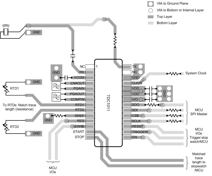
TDC1011-Q1 layout_rec_NAS648.gifFigure 57. TDC1011 Board Layout (Capacitive Feedback Mode)